Ray Wilson authored this content while he was actively running MFOS as the founder and resident genius.
We retain the content because it reflects a valuable point of view representing that time and place.
Article by Ray Wilson
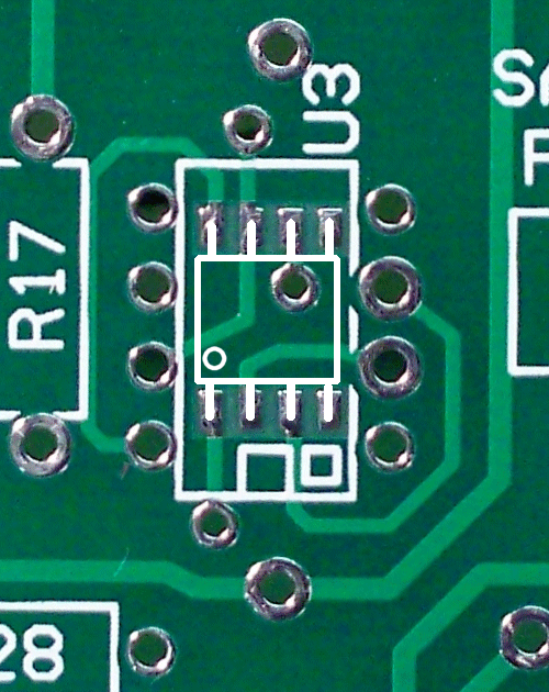
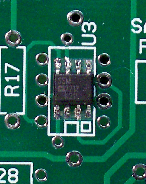
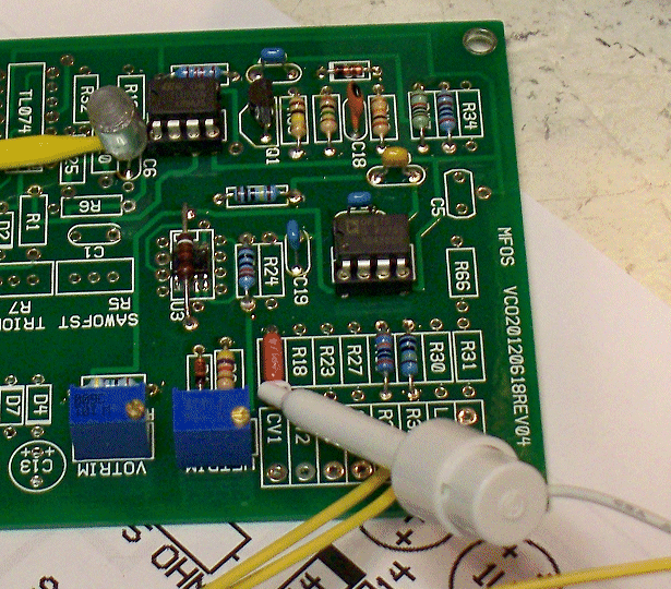
There has been a board layout change to allow the board to accomodate either a pair of matched discrete transistors, or an 8 pin DIP package for SSM2210 or LM394 dual transistors or an 8 pin surface mount SOIC package for SSM2210 and SSM2212. You REALLY have to be a good at soldering to solder a SOIC package so please don't make this your maiden voyage just in case. I do it under a magnifier with a sharp chiseled soldering tip and thin rosin core solder. If you don't need a magnifier to solder SOICs then vision is your super power in case you hadn't discovered it yet. Additionally R11 changed from 20K to 100K trimmer potentiometer to aid in high frequency trimming.
Features
MP3 SamplesSine wave with sequencer and keyboard Sine wave with sequencer and keyboard Triangle wave with sequencer and keyboard Ramp wave with sequencer and keyboard Square/Pulse with sequencer and keyboard Sync Effects Frequency Range Demonstration Modulation with keyboard and LFO Messing about with ramp waves (3 VCOs) Messing about with square waves (3 VCOs) Messing about with the sequencer attached (4 VCOs) Messing about with the sequencer attached (4 VCOs)Links to previous versions for reference |
|
Introduction
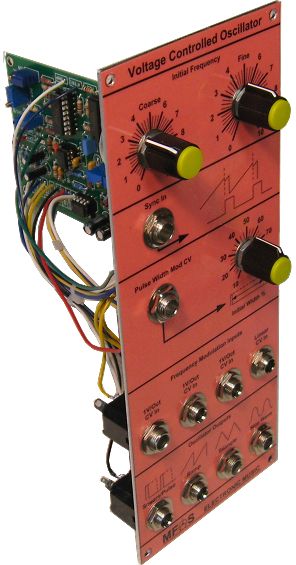
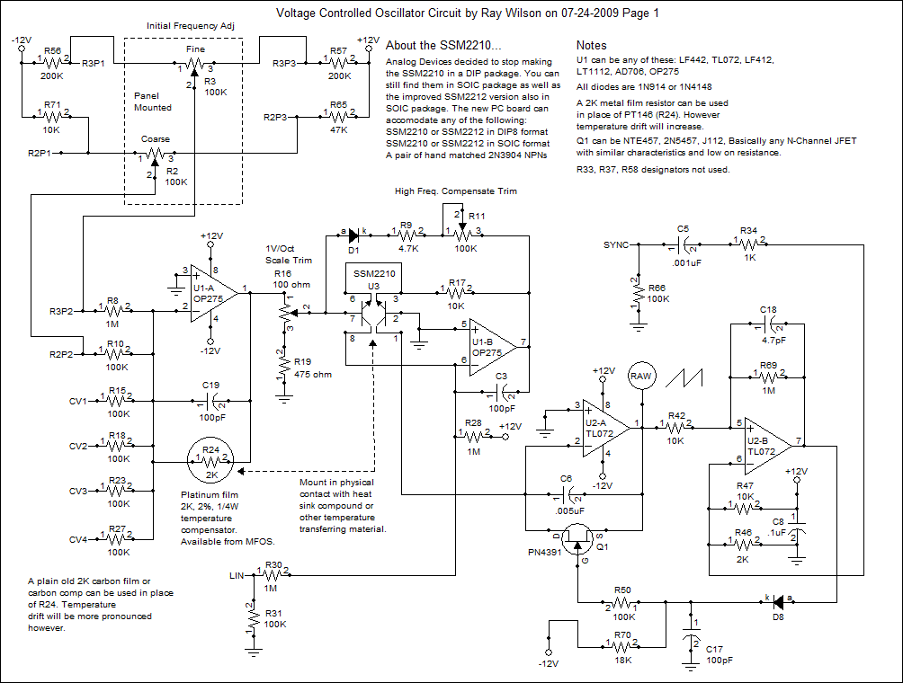
Oscillators are the main tone generating modules of your synthesizer. This oscillator produces sine, square, triangle and ramp waveforms and with careful adjustment tracks at 1V/octave over 6 to 8 octaves. The parts for it are easily obtained and not extremely expensive. The whole circuit is here so breadboard it and see if you like it. I like this oscillator but please recognize that it relies on a well matched pair of transistors. Its frequency range is from below audible to beyond audible. If this oscillator meets your needs I have high quality PC boards for sale for this design.Voltage Controlled Oscillator Schematic Page 1 PDF
While helping diyer Doug Slocum improve the tracking on his MFOS VCOs I found a few things +/-15V users should change.
- Change R46 to 1.54K metal film (1.5K carbon will be ok too). This sets the bias for the comparator since it changes at +/-15V. This corrects the whole rest of the waveform chain's amplitude.
- Change R10 to 150K and R65 to 43K this will give you a better range on the coarse freq control. Use metal film.
- Change R28 to 1.5M metal film. Changes the starting current of the expo convertor to 1uA.
- Use OP275 for U1. Its performance is superior to other op amps.
- Make sure and use a 100K multi-turn for the high frequency adjust.
| Approx. Current Consumption | |
| +12V | 28mA |
| -12V | 26mA |
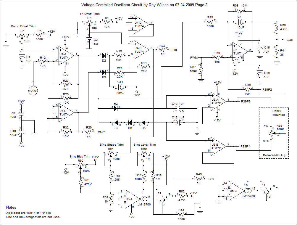
Voltage Controlled Oscillator Schematic Page 2 PDF
While putting together a few oscillators recently I changed R68 to 1M and got a much wider range of pulsewidth adjustment. However, in the extreme settings (all the way up or all the way down) it could cause the pulse wave to cease output. I don't mind this as it lets me set very narrow pulse widths.


Voltage Controlled Oscillator Scale Calibration
After getting the waveforms adjusted properly you need to set the oscillator scale factor and high frequency compensation trim pots. You will need a stable adjustable voltage source that can provide 0 through 10 volts, an accurate DVM, and a frequency counter. You can use an oscilloscope instead of the frequency counter but the frequency counter is more accurate. Without a frequency counter or scope you will need to use your ears. The following process is iterative and can be tedious. If you have a keyboard controller or MIDI to CV convertot that puts out 1V/octave I find it is easier to simply play octaves on the keyboard and trim the scale factor and high frequency compensator until I get the correct 1V/octave response.- Adjust the waveforms properly as described above.
- Connect the square wave output to your frequency counter.
- (Optional) Connect the sine wave output to an amplifier to listen as you go.
- Adjust R11 so that you have the most resistance between its pin 2 and pin 3 and thus the least high frequency pitch correction. We will adjust this later as necessary.
- Apply an adjustable voltage source to one of the 1V/Oct CV inputs.
- ITERATION POINT A
- Set the adjustable voltage source connected to the 1V/Oct CV input up to 0.000 volts.
- Adjust R2 and R3 so that the oscillator frequency is 100 Hz.
- Set the adjustable voltage source connected to the 1V/Oct CV input up to 3.000 volts.
- Observe the new frequency (which should be 800 Hz).
- If the observed frequency is 800 hz continue to "ITERATION POINT B"
- If the observed frequency is higher adjust R16 (Scale Adjust Trimmer) to cause the frequency to go higher. If the observed frequency is lower adjust R16 (Scale Adjust Trimmer) to cause the frequency to go lower. Repeat from "ITERATION POINT A"
- ITERATION POINT B
- Set the adjustable voltage source connected to the 1V/Oct CV input up to 3.000 volts.
- Adjust R2 and R3 so that the oscillator frequency is 800 Hz.
- Set the adjustable voltage source connected to the 1V/Oct CV input up to 6.000 volts.
- Observe the new frequency (which should be 6400 Hz).
- If the observed frequency is 6400 hz continue to "CALIBRATION COMPLETE"
- If the observed frequency is flat adjust R11 to cause the frequency to go to 6400 Hz.
- CALIBRATION COMPLETE

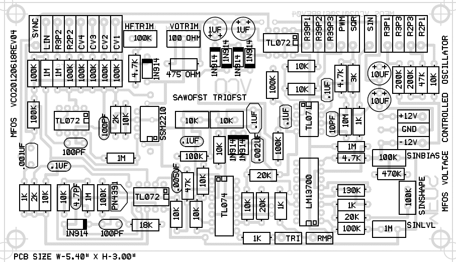
A SOIC style package can be used for the dual transistor chip on the new VCO board layout Soldering a SOIC chip is DIFFICULT and it is VERY easy to bridge the pads. Use a fine tipped soldering iron (I prefer a fine chisel point) and very thin solder and very little of it.
Here are some YouTubes that give some tips on soldering surface mount components. Glean what you can and remember that the drag soldering technique relies on having first applied flux as shown in the vids. You can definitely solder the part with your regular small tipped soldering iron but as they show first tack two opposite corner legs down. Take your time, use a magnifier, use VERY LITTLE solder, and have your desolder braid handy for removing any excess.
- Norman Mier of BEST, Inc.
- SMT Hand Soldering - Surface Mount SOIC IC
- Professional Hand Soldering (Basic to Advance) - Surface Mount, Through-Hole, Wires & Terminals
| This is how to orient the SOIC package. There is no legend on the PC board for it. | This is after soldering (I could have used less solder). I had to wick away some solder when I bridged two adjacent pads. |
 |
 |
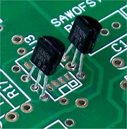
Two matched 2N3904 transistors can be used on the board for the linear voltage to exponential current convertor.
MFOS sells a package with two matched transistors and a temperature compensator.
MFOS sells a package with two matched transistors and a temperature compensator.
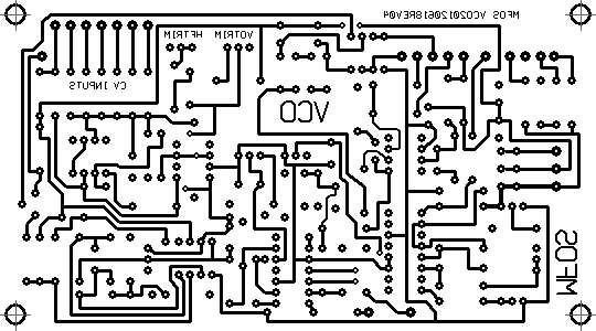
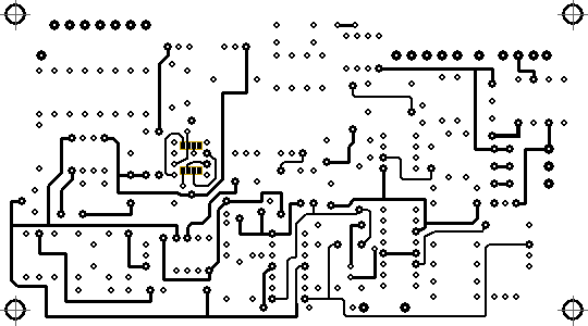
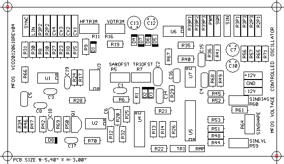
Voltage Controlled Oscillator PCB Layouts
Voltage Controlled Oscillator Front Panel Drawings and Wiring
Voltage Controlled Oscillator Front Panel PDF| This overlay fits the UNIVERSAL panels specified on this page. |
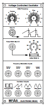
| Dave Kronemeyer took the time to make a nice Front Panel Express design and share it with all of us. If you use it make sure you take into account any differences related to the wiring diagram. | ||
|

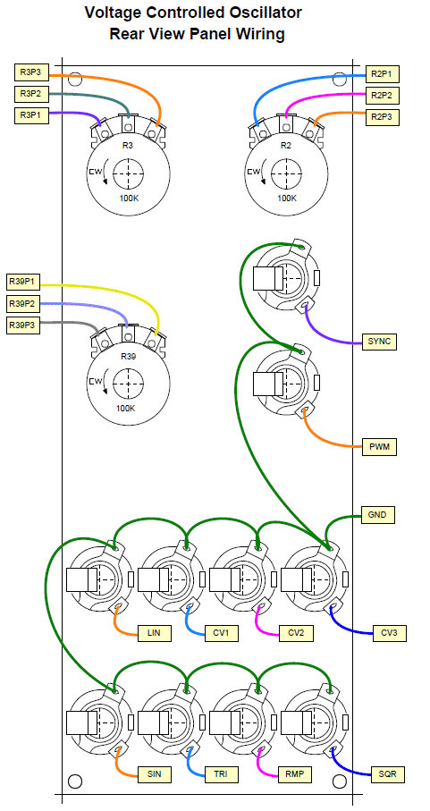
Voltage Controlled Oscillator Back Panel PDF
Voltage Controlled Oscillator Project Parts List
Order enough DIP sockets for ALL chips. Sockets are your friends!
Capacitor voltage rating should be 25V or greater for all capacitors.
Non-electrolytic capacitors can be film or ceramic type.
The integrator cap (C6 .005uF) needs to be temperature stable
so buy silvered mica, polystyrene or polycarbonate.
OP275 - LT1112, AD706, LF442, TL072
AD SSM-2210 - LM394 DIP or Two matched transistors (specs similar to 2N3904)
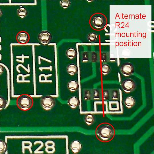
R24 (metal film 2K Ohm 1/4W +/-2% T.C. +3300 PPM tempco) - 2K Carbon Comp Resistor (provides no temperature compensation)
LM13700 - LM13600, NE5517, AU5517, NTE870, NJM13600D
TL074 - Any quad JFET op amp
PN4391 - 2N5457, J210, NTE457
MFOS sells a pack of 5 brand new Fairchild 2N5457 N-Channel JFETs and a pack of 5 brand new Fairchild PN4391 N-Channel JFETs
I suggest using 1% metal film for all resistors shown on page 1 of the schematic. Using 1% metal film for all resistors shown on page 2 of the schematic except for R68 (10M) and R22, R26, R34, R49, R51 (1Ks) will give greater uniformity of operation among multiple VCOs and better temperature tolerance but 5% carbon film resistors can be used as well.
| Qty. | Description | Value | Designators |
|---|---|---|---|
| 1 | LM13700 Dual gm OpAmp See notes above for subs. | LM13700 | U5 |
| 1 | OP275 Dual BiFET Op Amp See notes above for subs. | OP275 | U1 |
| 1 | SSM2210 Matched NPN Pair See notes above for subs. | SSM2210 | U3 |
| 1 | TL071 Op Amp | TL071 | U7 |
| 2 | TL072 Dual Op Amp | TL072 | U2, U6 |
| 1 | TL074 Quad Op Amp | TL074 | U4 |
| 1 | PN4391 N Channel JFET See notes above for subs. | PN4391 | Q1 |
| 8 | High Speed Switching Diode | 1N914 | D1, D2, D3, D4, D5, D6, D7, D8 |
| 3 | Linear Taper Potentiometer | 100K | R2, R3, R39 |
| 2 | Metal Film 1/4 Watt 1% Resistor | 2K | R24, R46 |
| 2 | Metal Film 1/4 Watt 1% Resistor | 47K | R20, R65 |
| 1 | Metal Film 1/4 Watt 1% Resistor | 475 ohm | R19 |
| 1 | Metal Film 1/4 Watt 1% Resistor | 470K | R61 |
| 3 | Metal Film 1/4 Watt 1% Resistor | 4.7K | R9, R36, R52 |
| 1 | Metal Film 1/4 Watt 1% Resistor | 3K | R41 |
| 12 | Metal Film 1/4 Watt 1% Resistor | 100K | R6, R10, R15, R18, R23, R27, R29, R31, R44, R50, R66, R67 |
| 11 | Metal Film 1/4 Watt 1% Resistor | 10K | R1, R12, R13, R17, R25, R32, R35, R40, R42, R47, R71 |
| 1 | Carbon Film 1/4 Watt 5% Resistor | 10M | R68 |
| 1 | Metal Film 1/4 Watt 1% Resistor | 130K | R53 |
| 1 | Metal Film 1/4 Watt 1% Resistor | 18K | R70 |
| 5 | Carbon Film 1/4 Watt 5% Resistor | 1K | R22, R26, R34, R49, R51 |
| 5 | Metal Film 1/4 Watt 1% Resistor | 1M | R8, R28, R30, R45, R69 |
| 2 | Metal Film 1/4 Watt 1% Resistor | 200K | R56, R57 |
| 3 | Metal Film 1/4 Watt 1% Resistor | 20K | R14, R21, R48 |
| 1 | Top Adjust Multi-Turn Trim Pot | 100 ohm | R16 |
| 3 | Top Adjust Multi-Turn Trim Pot | 100K | R11, R60, R64 |
| 2 | Top Adjust Multi-Turn Trim Pot | 10K | R5, R7 |
| 1 | Top Adjust Multi-Turn Trim Pot | 1M | R59 |
| 1 | Ceramic Capacitor | 10pF | C4 |
| 3 | Ceramic Capacitor | 100pF | C3, C17, C19 |
| 5 | Ceramic Capacitor | .1uF | C1, C2, C8, C15, C16 |
| 1 | Ceramic Capacitor | .002uF | C14 |
| 1 | Ceramic Capacitor | 4.7pF | C18 |
| 1 | Ceramic Capacitor | .001uF | C5 |
| 2 | Electrolytic Capacitor | 10uF 25V | C7, C10 |
| 1 | Silvered Mica, Polycarbonate or Polystyrene Cap | .005uF | C6 |
| 2 | Tantalum Capacitor | 1uF 25V | C12, C13 |
- (1) 4" x 10" 1/16" thick Aluminum plate for mounting the pots and switches.
- Unit is typically mounted in a synth case with other synth modules.
- Assorted hardware 1" 6-32 nuts and bolts, 1/2" #8 wood screws, etc
- Knobs for potentiometers, wire, solder and typical assorted electronics hand tools.
- Digital Volt Meter and a Signal Tracer or oscilloscope for testing.