Ray Wilson authored this content while he was actively running MFOS as the founder and resident genius.
We retain the content because it reflects a valuable point of view representing that time and place.
Article by Ray Wilson
Features
|
|
|
|
|
MP3 SamplesSine wave with sequencer and keyboard Sine wave with sequencer and keyboard Triangle wave with sequencer and keyboard Ramp wave with sequencer and keyboard Square/Pulse with sequencer and keyboard Sync Effects Frequency Range Demonstration Modulation with keyboard and LFO |
|
Introduction
Oscillators are the main tone generating modules of your synthesizer. This oscillator produces sine, square, triangle and ramp waveforms and with careful adjustment tracks at 1V/octave over a very useful range. The parts for it are easily obtained and not extremely expensive. The whole circuit is here so breadboard it and see if you like it. I like this oscillator but please recognize that it relies on a well matched pair of transistors. Its frequency range is from below audible to beyond audible but its tracking performance degrades above about 4 to 5 KHZ. However notice this chart of frequency ranges for vocals and instruments: Interactive Frequency Chart - Independent Recording Network. If this oscillator meets your needs I have high quality PC boards for sale for this design.
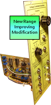
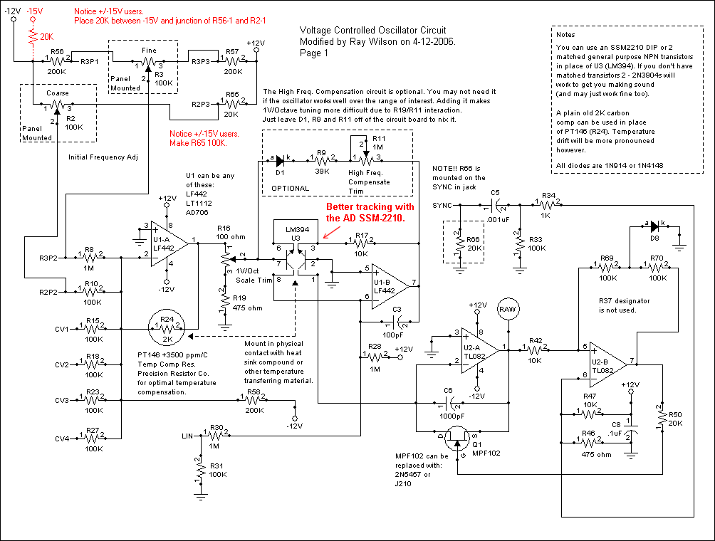
Voltage Controlled Oscillator Page 1 PDF
Coarse Frequency Range Customization
In order to customize the range of the Coarse frequency pot to your needs you can place a resistor in the range of 10K to 47K between the Coarse frequency pot terminal connected to -V and -V (RN in the illustration). The lower the resistor's value the lower the frequency will be on the low side of the Coarse frequency adjust's range.
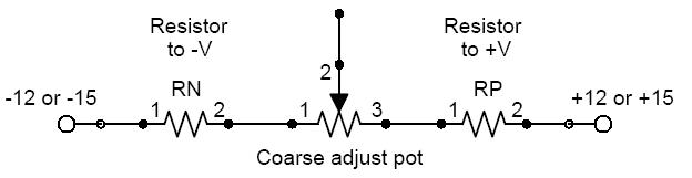
You can also increase the value of the resistor between the Coarse frequency pot terminal and +V to decrease the max frequency at the highest setting of the Coarse frequency pot (RP in the illustration). Note that changes in any of the values will cause interaction since the three of them form a resistive divider. These values will differ for people using +/-12V or +/-15V. Values on the high side resistor can go to 100K and on the low side to 20K for +/-15V users. Values on the high side resistor can go to 68K and on the low side to 10K for +/-12V users. Other values for RN and RP will not hurt anything as long as you keep the value of the Coarse frequency pot at 100K. at least
|
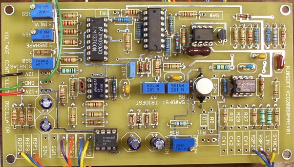
Page 1 shows the voltage to exponential current conversion and ramp generator circuitry. U1-A is the control voltage summer. It's output
feeds the scale trimmer R16 whose wiper is connected to the base of the current reference transistor in the feedback loop of U1-B.
Linear changes in voltage applied to the CV1 through CV4 inputs of U1-A are converted to logarithmic changes in current
at the current sink (collector of NPN transistor at pins 1(c), 2(b) and 3(e) of the LM394 Super Matched Pair IC).
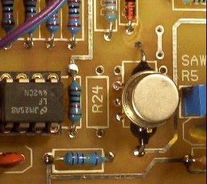
The optional high frequency compensation circuitry D1, R9 and R11 allow the output of U1-B to boost the current at the current sink at higher control voltage (and thus higher frequency) to make up for the finite time required to discharge the integration capacitor C6 during oscillation. Only add these components if the oscillator goes flat at high frequencies after you have adjusted the V/Octave scale trimmer. The interaction between the scale trimmer and the high frequency compensation can be challenging to adjust. The current sink causes the integrator made up of U2-A and C6 to ramp from ground toward V+. The comparator (made up of U2-B and associated components) dashes the hopes of U2-A reaching V+ by causing the integrator cap to discharge when it detects a level higher than approximately 1.1 volts. This happens when the comparator's output goes high turning on Q1. R47 and R46 hold +0.544 volts at the non-inverting input of U2-B. This level plus the approximately +0.5 volts required to overcome the hysteresis provided by R42 and R37 is what determines the threshold of the comparator. Thus the output of U2-A (point RAW) is a ramp wave that goes from ground to +1.1 volts. The fall time of the ramp is approximately 1uS. The output of U2-B is a very brief pulse (ALWAYS use the x10 setting on your probe to observe it) that goes from -V to just above ground and then back to -V. It is about 1.5 uS in duration. The ramp's frequency is determined by the control voltage applied to the CV1 through CV4 inputs with a conversion of 1V per octave. This is the heart of the VCO (literally). Applying a control voltage to the LIN input causes a linear shift in frequency as this input affects the reference current in the exponentiator. Applying a square wave from another oscillator to the sync input causes the comparator to reset the integrator (on the rising edges of the square wave) which produces interesting timbres when the outputs of the oscillator providing the sync signal and the oscillator being synced are mixed. Panel mounted pots R2 and R3 provide the initial frequency (tuning) adjustment. Detailed setup instructions are in a section below. R16 and R11 (if used) should definitely be multi-turn cermet type trim pots so you have fine resolution when adjusting the V/Oct scale and high frequency compensation. These ideas were pioneered by the Alan Pearlmans, Bernie Hutchins, and Bob Moogs of the world I am merely a student of their landmark work. For best performance and least temperature drift use: 1% resistors throughout this portion of the circuitry, a PT146 TCR for R24, and a silver mica or polystyrene capacitor for C6. If you use the PT146 TCR for R24 you need to put it in direct thermal contact with the matched transistors used in the exponentiator. The board is designed to accomodate a wide range of transistors from the LM394 to two separate transistors. I ended up mounting my TCR first and then putting some heat sink grease on top of that, followed by the 6 pin can-type LM394 straddling the TCR so that its silica substrate is contacting the TCR and heat sink grease. You can substitute some of the parts as listed at the beginning of the parts list section below. |
Voltage Controlled Oscillator Page 2 PDF
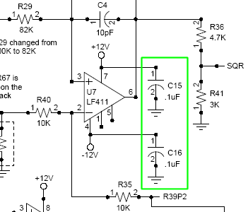
Rev two boards have these two caps on them.
Boy are our faces red. The output marked SAW on the PC board is actually... a ramp wave. What was that...? it's a ramp wave. Come again... alright alright I said it's a RAMP WAVE. Somehow in all the confusion the last inversion got missed and we marked it as a Sawtooth. So consider this an embarassing moment and lets all move on.
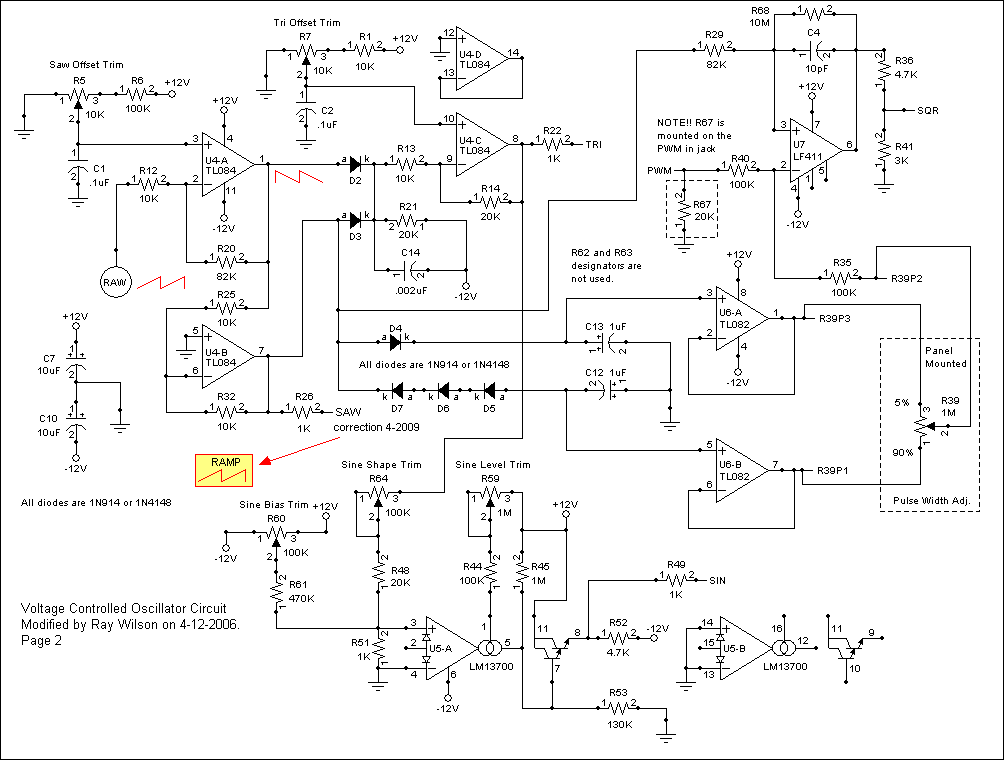
Page two shows the circuitry that converts the raw ramp wave into ramp, triangle, sine, and rectangle waveforms. RAW is applied
to inverting buffer U4-A where gain and offset are applied to the signal. The original 1.1 volt signal is boosted to about
8.5 volts P-to-P. Adjust R5 so that the sawtooth waveform at pin 1 of U4-A oscillates evenly about ground.
|


Voltage Controlled Oscillator Adjustment
|
After getting the waveforms adjusted properly you need to set the oscillator scale factor and high frequency
compensation trim pots. If used, adjust R11 so that you have the most resistance between its pin 2 and pin 3
and thus the least high frequency pitch correction. We will adjust this later as necessary.
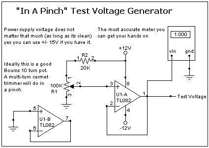
Adjust R2 and R3 so that the oscillator frequency is 100 Hz. You will need to apply a calibrated voltage at one of the CV inputs starting at GND and then increasing the voltage to exactly 1.000V, 2.000V, 3.000V, 4.000V, 5.000V... etc. In a pinch you can use this circuit to provide test voltage.
If you start to find that the octaves are in tune to a certain point but then start getting flat at the next higher voltage level then its time to adjust R11 to compensate a bit because at high frequency you need the oscillator to give a smidge more than 1 octave per volt response. At the step where the frequency is flat adjust R11 to raise the pitch. You will need to go back and restest & readjust at all voltages if you introduce pitch correction via R11 as there is some interaction between R16 and R11. It's best to use a frequency counter to measure but your ears will work fine. Adjust the oscillator to the best of your ability and over the audio range you are most interested in. I suggest 100 to 6400 hz. You will certainly hear harmonics and overtones at frequencies well above this but I suggest these 6 octaves as the sweet spot for the oscillator tracking. |
Board Revisions
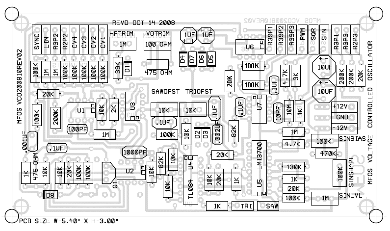
Rev October 2008 boards have some slight layout changes and the addition of R66 and R67. These will no longer need to mounted on the
Sync In or PWM jacks respectively.
October 2008 boards say "REVD Oct 14 2008" on them.
Part Value View
Rev 2 boards have some slight layout changes and the addition of C15 and C16 .1uF U7 bypass caps.
Rev 2 boards say "MFOS" instead of "RJWSOFT".
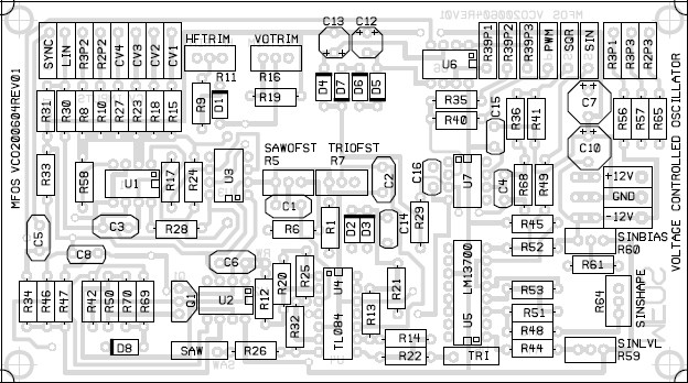
Part Value View
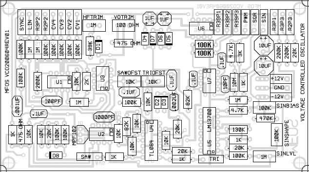
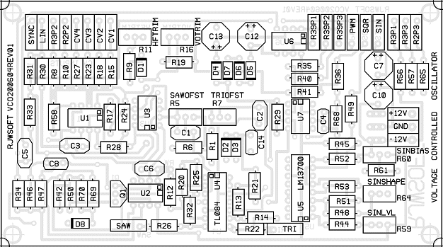
Rev 1 boards
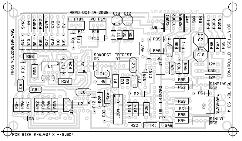
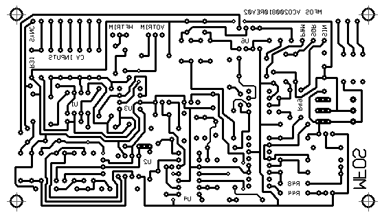
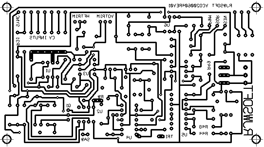
Voltage Controlled Oscillator PCB Parts Layout (Parts Side Shown) PDF
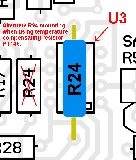
Alternate placement of R24 When using a PT146 (or equivalent) tempco
|
Notice that there is a legend for R24 but there are two alternate mounting holes on the board specifically for
mounting a PT146 Tempco for R24 so that it is in thermal contact with U3 (or replacement transistors). Use thermal
grease or epoxy to make the thermal contact. The Tempco can go above or below the LM394 depending on the package you buy.
It can go in between discrete transistors if you use those instead of a dual transistor package.
IMPORTANT INFORMATION! You should only install one of the resistors. If you use the PT146 Tempco
for R24 in the alternate mounting then do not mount the regular R24. Otherwise your oscillator scaling will be off by a
factor of 2 (i.e. an octave will span 2 keyboard octaves).
|
|
|
|
Board Revisions
Rev October 2008
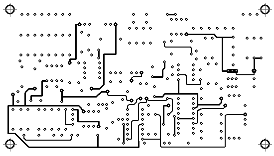
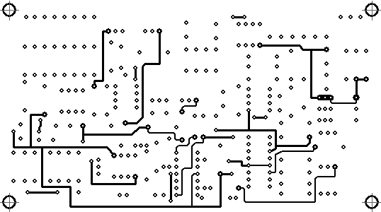
Voltage Controlled Oscillator PCB Bottom Copper (Parts Side Shown)
Voltage Controlled Oscillator PCB Top Copper(Parts Side Shown)
Rev 2
Voltage Controlled Oscillator PCB Bottom Copper (Parts Side Shown)
Voltage Controlled Oscillator PCB Top Copper(Parts Side Shown)
Voltage Controlled Oscillator Front Panel PDF
| I always work with these non-standard 10 x 4 x 1/16" aluminum panels because I get them for $2.50 each. You can certainly change the front panel to whatever you like but make sure you wire it up correctly. |
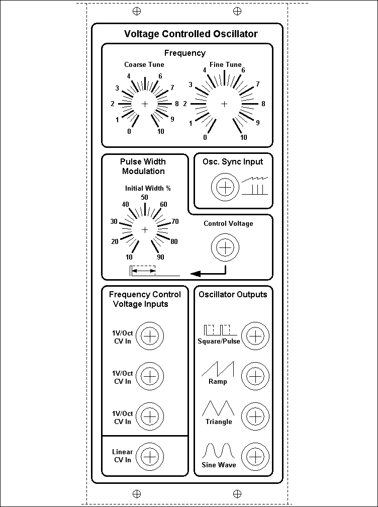
| Dave Kronemeyer took the time to make a nice Front Panel Express design and share it with all of us. If you use it make sure you take into account any differences related to the wiring diagram. | ||
|

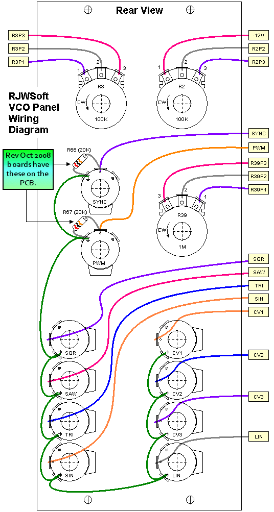
Voltage Controlled Oscillator Back Panel PDF
Voltage Controlled Oscillator Project Parts List
|
Substitutions
LF442 - LT1112, AD706
|
VCO Project Parts List
| Qty. | Description | Value | Designators |
|---|---|---|---|
| 1 | LF411 Op Amp | LF411 | U7 |
| 1 | LF442 Dual Op Amp | LF442 | U1 |
| 1 | LM13700 Dual gm OpAmp | LM13700 | U5 |
| 1 | LM394 Super Match Pair AD SSM-2210 (Preferred) | LM394 | U3 |
| 2 | TL082 Dual Op Amp | TL082 | U2, U6 |
| 1 | TL084 Quad Op Amp | TL084 | U4 |
| 1 | MPF102 | MPF102 | Q1 |
| 8 | High Speed Sw Diode | VALUE | D1, D8, D2, D3, D4, D7, D5, D6 |
| 1 | Ceramic Capacitor | .001uF | C5 |
| 5 | Ceramic Capacitor | .1uF | C8, C2, C1 |
| 1 | Ceramic Capacitor | 100pF | C3 |
| 1 | Ceramic Capacitor | 10pF | C4 |
| 2 | Electrolytic Capacitor | 10uF | C7, C10 |
| 2 | Tantalum Capacitor | 1uF | C13, C12 |
| 1 | Ceramic Capacitor | .002uF | C14 |
| 1 | Silvered Mica or Polystyrene Cap | 1000pF | C6 |
| 2 | Potentiometer | 100K | R2, R3 |
| 1 | Potentiometer | 1M | R39 |
| 1 | Trim Pot 10 Turn | 100 ohm | R16 |
| 1 | Trim Pot 10 Turn | 1M | R11 |
| 2 | Trim Pot Single Turn | 100K | R60, R64 |
| 2 | Trim Pot Single Turn | 10K | R7, R5 |
| 1 | Trim Pot Single Turn | 1M | R59 |
| 13 | Resistor 1/4 Watt 1% | 100K | R15, R18, R10, R31, R23, R27, R33, R69, R70, R44, R40, R35, R6 |
| 8 | Resistor 1/4 Watt 1% | 10K | R17, R42, R47, R13, R25, R32, R12, R1 |
| 1 | Resistor 1/4 Watt 5% | 10M | R68 |
| 1 | Resistor 1/4 Watt 1% | 130K | R53 |
| 5 | Resistor 1/4 Watt 1% | 1K | R34, R51, R49, R26, R22 |
| 4 | Resistor 1/4 Watt 1% | 1M | R30, R8, R28, R45 |
| 3 | Resistor 1/4 Watt 1% | 200K | R56, R57, R58 |
| 7 | Resistor 1/4 Watt 1% | 20K | R50, R65, R66, R14, R21, R48, R67 |
| 1 | Resistor 1/4 Watt 1% | 2K | R24 |
| 1 | Resistor 1/4 Watt 1% | 39K | R9 |
| 1 | Resistor 1/4 Watt 1% | 3K | R41 |
| 2 | Resistor 1/4 Watt 1% | 4.7K | R52, R36 |
| 1 | Resistor 1/4 Watt 1% | 470K | R61 |
| 2 | Resistor 1/4 Watt 1% | 475 ohm | R19, R46 |
| 2 | Resistor 1/4 Watt 1% | 82K | R20, R29 |
Miscellaneous
- (1) 4" x 10" 1/16" thick Aluminum plate for mounting the pots and switches.
- Unit is typically mounted in a synth case with other synth modules.
- Assorted hardware 1" 6-32 nuts and bolts, 1/2" #8 wood screws, etc
- Knobs for potentiometers, wire, solder and typical assorted electronics hand tools.
- Digital Volt Meter and a Signal Tracer or oscilloscope for testing.