8 Channel Expandable Analog Sequencer (PC Board and How to Expand)
8 Channel Expandable Analog Sequencer Schematic
The main idea of a sequencer is to provide an automatic means of sequentially stepping through a series of adjustable voltages to drive a VCO (or any other voltage controlled device). Additionally, gate and trigger signals are generated at the moment the output of the circuit steps to a new voltage. Typically you use a sequencer to control the frequency of an oscillator (or several oscillators) to produce repeating tonal patterns, or arpeggios, which are further enhanced by filtering, modulation, addition of keyboard voltage etc. Sequencers are often used in electronic music production.
IMPORTANT!!!! You must insert a jumper onto the board between "mstr" and "D" (these points are shown on the parts layout at the top of the parts layout image) in order for the circuit to function. I do not show this jumper installed on the parts layout.
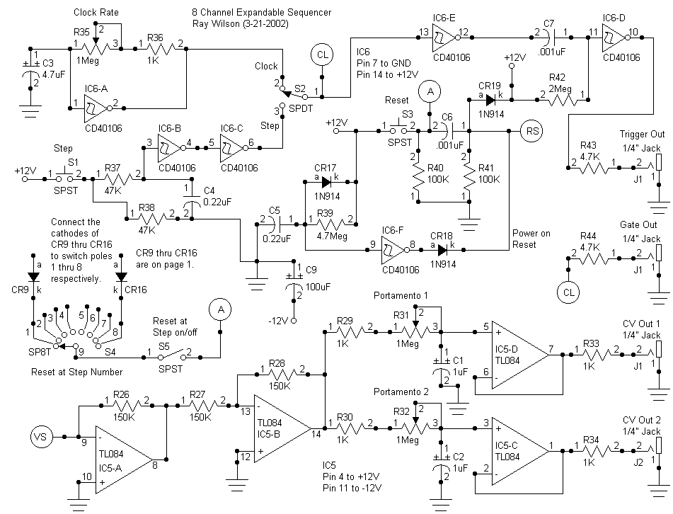
Starting with page 2 (sorry about that) Schmitt inverter IC6-A and associated comps (R35, R36, and C3) form a square wave oscillator that is used to drive the sequencer and as the gate/trigger signal source. When IC6-A pin 2 is high it charges C3 via R35 and R36 in series until the upper threshold of IC6-A is reached at which point pin 2 IC6-A goes low and begins to discharge C3 until it gets below the lower threshold of IC6-A and its output flips back high. This cycle repeats producing oscillation at pin 2 of IC6-A. This signal is used to clock the sequencer. IC6-E, IC6-D and associated components (C7 and R42) are used in this manner. IC6-E inverts the clock/debounced step pulses and feeds them to differentiator C7/R42. IC6-D inverts and squares up the pulse arriving at its input (pin 11) to form the approximately 2mS trigger signals. R43 current limits the output from IC6-D to a safe level even if the trigger out is grounded (R44 does the same for the gate out).
IC6-B and IC6-C and associated comps (R37, R38 and C4) are used to debounce the action of S1 so that each depress-release cycle of S1 causes one square pulse to be emitted from IC6-C's output (pin 6). When S1 closes C4 charges via R37. When the voltage on C4 goes above IC6-B's upper threshold pin 4 goes low and subsequently IC6-C pin 6 goes high. When S1 is released C4 discharges through R37 and R38 and when the lower threshold of IC6-B is reached its output goes high (driving IC6-C's output low). Debouncing is important when you want to single step digital logic. This signal is used to manually step the sequencer. Without debouncing the chatter of S1's contacts closing/opening alone would cause an indeterminant number of clocks to be generated.
When building the circuit you should see a square wave at the Gate Out jack's hot when S2 is set to "Clock". You should be able to adjust the frequency of the square wave with pot R35. When you switch to "Step" you should see the Gate Out go high when you press S1 and then low when you release S2. You should see a corresponding trigger (2mS pulse) at "Trigger Out" for each low to high transition of the gate signal.
S3 is used to jam a pulse onto the reset line of the CD4013's used to generate the sequential action. It is not debounced because we really don't care how many reset pulses the reset line gets as long as it gets the message to RESET! The power on reset is necessary because when the circuit first powers up there is no telling what logic states the CD4013s will be at. So as power is applied, C5 (which had been previously discharged) is essentially low which causes IC6-F to put a hard high on the reset lines via CR18. After C5 charges via R39 IC6-F's output goes low and doesn't reset the CD4013s anymore (until the next power on).
When building the circuit you should monitor pin 8 while you apply power. Pin 8 should go high for a short period after power is applied and then go low.
OK now we know how the clock, step and reset signals get generated.
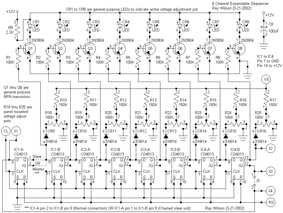
Page one shows the CD4013s used to generate the sequence. D-Flip Flops are very versatile little chips. In this circuit we are using them as follows: We ground the set and reset pins (we poke the reset high when we want to reset the circuit) so that they are out of the picture. The logic level present on the D input of a D-Flip Flop is transferred to its Q output when a clock signal (rising edge of a logic signal) is applied to the clock (CLK) input. The /Q (NOT Q) output assumes the logic level that is opposite of what is present on the Q output (they don't call it "NOT Q" for nothing). Anyway, the chips are wired in such manner that when the reset is pulsed all of the Q outputs are low, but note that the first position (IC1-A) (when used as Master) uses the /Q output so it is high. So on a reset the first position is "ON", its LED is lit and its pot is able to provide an adjustable voltage level. Also note that IC1-B through IC4-A all pass the Q output to the next flip-flop's D input. HOWEVER, note that the last position (IC4-B) passes its /Q back to IC1-A's D. So on reset: IC1-A's /Q is high, all the other D-Flip Flop's Q outputs are low. What happens when a clock signal is fed to all the clock inputs? Well... the high on IC1-A's /Q is transferred to IC1-B's Q output, the high that was on IC4-B's /Q is transferred to IC1-A's Q BUT NOTICE THAT WE USE IC1-A'a /Q output to feed its associated pot and LED so IC1-A'a /Q goes to the opposite level or LOW. The logic 1 now on pin 13 of IC1-B keeps getting shifted to the next flip-flop's Q as the circuit is clocked. All of the preceding Q's are getting a 0 shifted to them. Finally the one gets shifted to IC4-B's Q which causes its /Q to go low. On the next clock the low on IC4-B is shifted into IC1-A which causes its Q to go low BUT ITS /Q to go high and voila we have a high logic level that keeps circulating around the circuit which is just what we need for a sequencer. The high logic level starts at IC1-A pin 2 and progresses to IC1-B pin 13, IC2-A pin 1, IC2-B pin 13, IC3-A pin 1, IC3-B pin 13, IC4-A pin 1, IC4-B pin 13, and back to IC1-A pin 2 (as previously explained). As each pin in turn becomes high it assumes a voltage of 12V which forward biases its associated diode and drops 12V (minus one diode drop) across its associated potentiometer. The voltage dropped on the pot is adjusted via the wiper and fed via a summing resistor (150K) into IC5-A. The voltage is re-inverted by IC5-B and buffered by IC5-C and IC5-D. Portamento is introduced via R31, R32 and C1 and C2 respectively. Each output also drives a transistor to turn on an LED so that you know which pot you should be adjusting.
To test the analog portion do this: Turn all of the pots to the off (counter-clockwise) position. Turn the Portamento pots so that pin 2 is adjusted to the pin 1 position (essentially shorted). Feed a voltage into pin 9 of IC5-A via a 150K resistor. The same voltage should appear at these points: pin 14 of IC5-B, pin 7 of IC5-D and pin 1 of IC5-C. If you feed a square wave test signal (1Hz 2 volts Peak to Peak) into pin 9 of IC5-A via a 150K resistor you should see the same square wave at CV Out 1 and CV Out 2. As you advance portamento pot R31 the square wave signal at CV Out 1 should change shape i.e. the front side of the square wave should resemble a capacitive charge curve and the trailing edge should resemble a capacitive discharge curve. CV Out 2 should similarly change shape corresponding with advancement of R32.
The clock signal is used as the gate out for the sequencer and 2 mS trigger pulses are generated via IC6-E, C7, R42, and IC6-D. All outputs are protected via 1K resistors (4.7K resistors for gate and trigger) so that if outputs are grounded or shorted to other signals none of the chips wil fry.
If you need to reduce the range of voltage that the sequencer outputs just reduce the gain of IC5-A by placing a lower value resistor as its feedback resistor (R26). As it is each channel, is adjustable over about 11 volts which may be a bit coarse at 1V/Oct equipment. At 75K you'll get approximately 0 to 6 volts at 39K you'll get approximately 0 to 3.2 volts. You could add a switch to change the range.
The 8 position switch is used to determine how many steps you desire before resetting the sequencer. If you don't use it you'll get 8 steps all the time.
This is a primitive circuit but at least it gets you started on the road to analog sequencing. Extending several of these for more channels is pretty self explanatory. But as you can see you would send X2 to the next board's X1, remove J3 from the first and subsequent boards, and feed the final board's X3 back to the first board's X1. Also you would connect the first board's Master jumper but all subsequent board's Slave jumper.
Have fun.
Page 1
Page 2
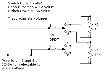
Modification to allow selectable full scale adjustment.