Ray Wilson authored this content while he was actively running MFOS as the founder and resident genius.
We retain the content because it reflects a valuable point of view representing that time and place.
Article by Ray Wilson
Table of Contents
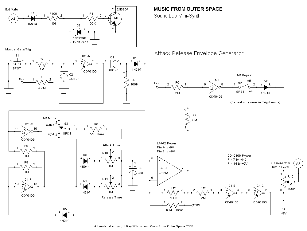
Sound Lab Mini-Synth AR (Attack - Release) Envelope Generator
| With S2 is in the off state and S3 set to "Trig'd" the circuit functions as follows. When S1 is momentarily pressed it discharges C2 (to about 1.6 volts) through R2 which causes
pin 2 of IC1-A to go high. This pushes a positive pulse through C1 and D1 which sets the flip flop made up of IC1-E and IC1-F. IC1-F pin 12 goes high and C3 begins to charge at the rate set by the
Attack pot R10 from -8 volts to about 6.5 volts (this voltage is buffered by IC2-B voltage follower) at which point IC1-B's output goes low and IC1-C's output goes high and the IC1-E/IC1-F flip flop
is reset by the high logic level presented to pin 13 via D5. This causes IC1-F pin 12 to go low and discharge C3 at a rate determined by R11.
When the Repeat switch is on and the voltage at IC2-B is lower than -6 volts then IC1-D pin 8 goes high and sets the IC1-E/IC1-F flip flop again thus causing the cycle to begin again and subsequently repeat. Notice that I am allowing negative voltages to reach the inputs of the schmidt triggers but that they are protected from drawing high current through their internal protection diodes during that time by the high value resistors in series with their inputs. When S3 is in the "Gated" position the repeat function is disabled. In this configuration a high level is presented to the "Attack" diode/pot combo as long as S1 is held pressed (because the output of IC1-A is high when S1 is held pressed). Gate mode allows C3 to charge from -8 volts to about +8 volts maximum. When S1 is released a low level is presented to the "Release" diode/pot combo (because the output of IC1-A is low when S1 is not pressed). The output of IC2-B is fed to R15, the AR Envelope output level adjustment pot. The circuit point "AR" is the wiper of R15, which is fed to the AR-Gen switches of the modules. While contemplating this circuit remember that the inverters are schmidt triggers and that their inputs must go lower than 1/3 of the supply voltage before their output goes high and then the input must go to greater than 2/3 of the supply voltage before the output goes low. This characteristic is know as hysteresis. The zener on the external gate is meant to protect against gate signals greater than 9 volts. When the gate is high transistor Q8 will discharge C2 the same way switch S1 does. NOTE: If you don't plan to use the external gate capability of the device you can eliminate the following components: D7, R199, R1, D8, Q8 NOTE: C2 has been changed from .01uF to .001uF to allow the AR generator to be triggered faster from external sources. |
Schematic PDF
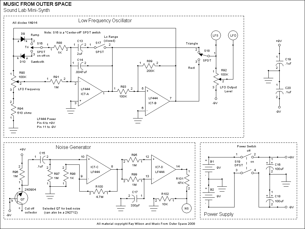
Sound Lab Mini-Synth LFO (Low Frequency Oscillator),
Noise Source, and +/- 9 Volt Battery Power Supply
Back to Top
| Two 2N3904s walk into a bar. One makes a lot of noise and gets thrown out, the other one sits and quietly drinks his stout. The punchline... some transistors are noisier than others. So how
do we get noise out of ANY 2N3904? With this circuit. Notice that we do the usual... reverse bias a low V(ebo) emitter base junction, listen to the junction through C10 and a gain of about 1000. If
this transistor is whispering it is still whispering into a lot of gain. This circuit does not care if this transistor is in a confessional you are going to get at least 100 mV of noise from the
first stage. We take whatever we are getting from the first LF444 and feed both inputs of a second LF444 through two 1M resistors. We hang a capacitor off of the inverting input and voila the
inverting input always lags the non-inverting one. As the noise voltage is taking its time trying to go up and down (due to the cap) on the inverting input it is racing up and down on the
non-inverting input. This results in the voltage on the non-inverting input randomly being higher or lower than the voltage on the inverting input as the noise voltage randomly changes. Since the
op-amp is wired as a full blast comparator its output is swinging up and down between the voltage limits of the LF444 in time to the noise fluctuations. Varying the cap and varying which input you
hang the cap on will change the characteristics of the noise at the output of the second stage.
The LFO is the same as the Super Simple Ramp and Sawtooth LFO. Notice that the switch is changed to be center off so the circuit produces a triangular wave too. This was suggested synth-DIYer Harry Bissell (I remembered the little email logo H^) that came with the suggestion.) thanks. Additionally, you can change the range of oscillation for the LFO with the range switch. In low range a 2uF cap (C13) is placed in parallel with the integrator capacitor (C14) to reduce the range of frequency provided by the Frequency pot R90. Two 9 volt batteries power the circuit and the two by-pass caps absorb the larger current spikes. I am planning on re-evaluating all of my circuits with the LF444 (low power op amp). These things are great. You get decent slew rates and much lower current consumption than with TL084s and TL082s. All of the circuits in the Sound Lab together draws less than 6mA. Hooking up two batteries for + and - 9 volts |
Schematic PDF
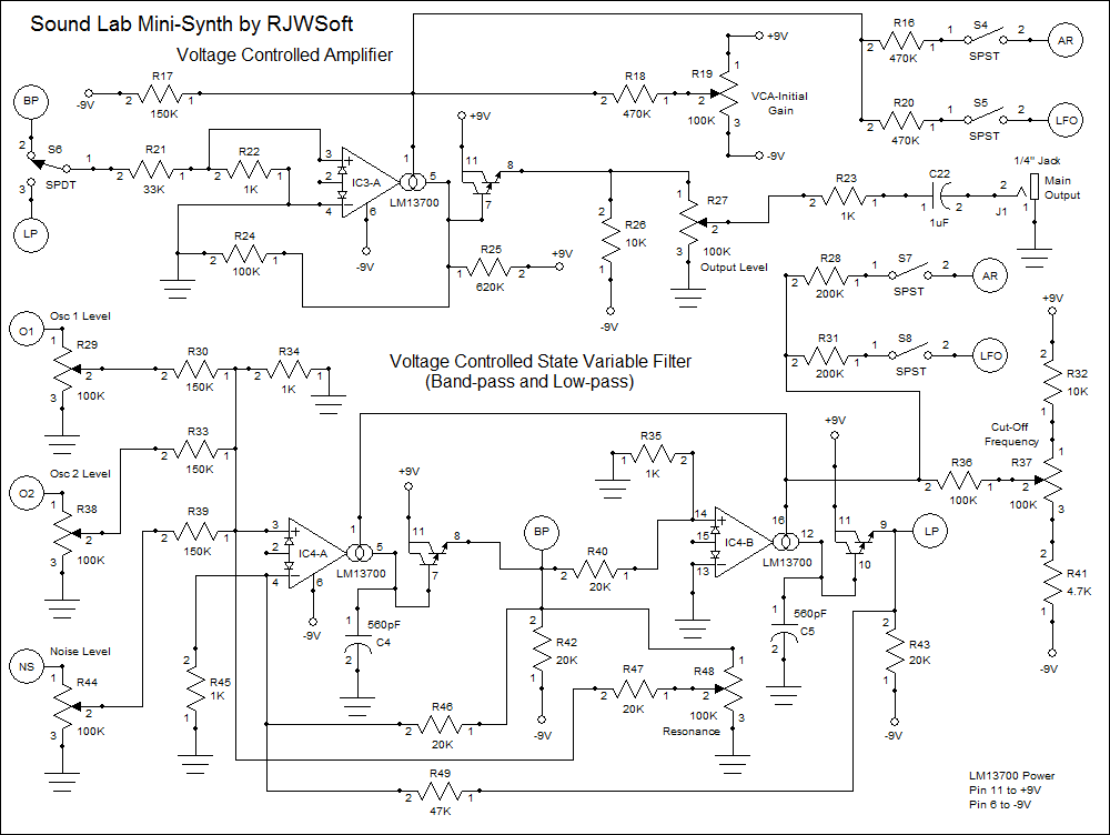
Sound Lab Mini-Synth VCA (Voltage Controlled Amplifier) and
VCF (Voltage Controlled Filter)
Back to Top
| These two circuits are practically straight out of the National Operational Amplifiers Databook data sheet for the LM13700. They have linear voltage control but for a sound box they're
fine. The transconductance characteristic of these Op Amps makes them perfect for VCAs and VCFs.
In the VCA the control voltage controls the current flow through the amp and subsequent level of the signal at the output. S4 switches the AR Gen control voltage on or off. When on, the level of the AR Generator output pot determines how much the AR Generator controls the signal amplitude at the output of the VCA. S5 switches the LFO control voltage on or off. When on, the level of the LFO output pot determines how much the LFO controls the signal amplitude at the output of the VCA. R19 controls the initial amplitude at the output of the VCA. When S4 or S5 is on it is best to turn R19 off or nearly off. In the VCF the OTAs act as voltage controlled resistors which change the pass-band (in band pass mode) and cut-off frequency (in low pass mode) from low (for low control voltage) to high (for high control voltage). The resonance control adjusts the feedback around the circuit and thus the gain at the cut-off frequency. At high resonance settings the filter rings adding harmonics to the filtered signal which give the classic synthesizer wahhhhh sound when the cut-off frequency is swept from low to high. The filter also acts as the mixer as all of the signal sources are presented to its input via attenuation pots (R29, R38, and R44). The input to the VCA is either the low pass output or the band pass output determined by the setting of switch S6. S7 switches the AR Gen control voltage on or off. When on, the level of the AR Generator output pot determines how much the AR Generator controls the cut-off frequency of the VCF. S8 switches the LFO control voltage on or off. When on, the level of the LFO output pot determines how much the LFO controls the cut-off frequency of the VCF. R37 controls the initial cut-off frequency of the VCF. When S7 or S8 is on it is best to turn R37 off or nearly off. |
Schematic PDF
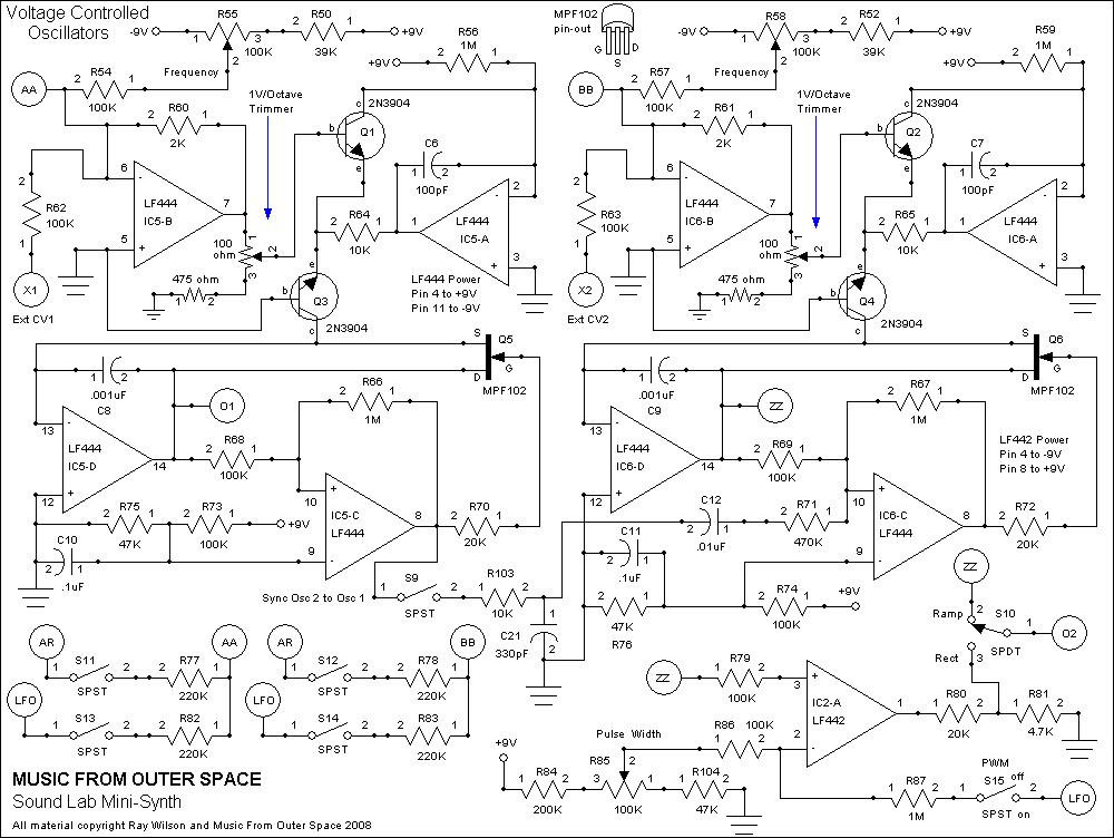
Sound Lab Mini-Synth VCOs (Voltage Controlled Oscillators) Rev 001
Back to Top| The sound lab uses two voltage controlled ramp oscillators. IC5-B and IC5-A and associated transistors and components comprise a linear voltage to logarithmic current convertor. The control
voltages which are summed by IC5-B range from -8 to 8 volts. The corresponding current ranges from around 1uA to 1mA and since the oscillators go up approximately 1 octave every time the current
doubles this gives the oscillator a nice range from a sub-audible 0.6 Hz to beyond human hearing (This is since changing the values of C8 and C9 to .001uF from .02uF)
The explanation of the operation of oscillator 1 follows (oscillator 2 works the same way using its associated components). Oscillation occurs because as the current is sucked out of the input of integrator IC5-D its output goes high until IC5-C (comparator with hysteresis) pin 8 goes high and turns on the N-Channel FET (Q5) which shorts the integrating capacitor (C8) which causes the cycle to begin anew and subsequently repeat. IC6 is used in a similar configuration. The output of IC6-D (point ZZ) is fed into comparator IC2-A in order to provide a square/pulse wave shaper for Oscillator 2. The control voltage fed into IC2-A pin 2 via resistors R86 and R87 determine the comparator threshold and thus the point at which the output (pin 1) goes high and low. Varying R85 will change the pulse width which will vary the timbre of Oscillator 2 when Rect Wave is selected. S15 permits the LFO output voltage to modulate the pulse width which can cause the output of Oscillator 2 to sound like 2 oscillators tuned very close together (when approximately 1HZ LFO frequency is used). S11, S13, S12, and S14 are used to feed the AR Generator and LFO outputs to the CV inputs of the VCOs. When on, you will hear the obvious effect as you advance the LFO and/or AR Gen output adjustments. S9 causes Oscillator 2 to sync to the frequency of Oscillator 1. This provides some very cool timbres which you will hear if you turn on Sync and then tune Oscillator 1 lower than Oscillator 2 and sweep Oscillator 1 upward in frequency. NOTES: If you don't plan to use the external CV (Control Voltage) capability of the device you can eliminate the following components: R62 and R63. To obtain the most accuracy of scaling of the oscillators for control via Ext CV1 and Ext CV2 do as many of the following mods as possible:
Oscillator CalibrationWhile the Sound Lab is primarily a sound generator and the oscillators are not stable or precision enough for many octaves of "in tune" 1V/octave range they can be calibrated so that you get an octave or two of "in tune" 1V/Octave range.
Revision 001 DescriptionReduced the value of the integrator cap for the VCOs from .02uF to .001uF. This changes the range of the oscillator so that it attains a higher top frequency and allows the integrator cap to discharge 20 times faster. Since the oscillator is inherently higher in pitch the wiring of the "Frequency" pots was changed so that the voltage at the wipers of R55 and R58 is able to go lower when turned all the way down and not as high when turned completely up. The oscillators will still go sub-audio (a few hertz) to beyond hearing (18 to 20 KHz). Additionally the sync works better since the integrator can be reset with a shorter pulse than before. The panel wiring diagrams have been updated to reflect the change. Replace C8 and C9 with .001 uF caps (temperature stable type) and rewire pots R55 and R58 on the front panel. Remember that R50 and R52 are not only moved as shown in the panel wiring diagram but that their values change to 39K.
|
Schematic PDF