Ray Wilson authored this content while he was actively running MFOS as the founder and resident genius.
We retain the content because it reflects a valuable point of view representing that time and place.
Article by Ray Wilson
This is an intermediate to advanced project and I do not recommend it as a first project if you are just getting started in synths or electronics. Only the circuit and some explanation are shown here. A lot of project building, troubleshooting and electronics experience is assumed. Additionally, electronic equipment ownership (scope, meters, etc.) is taken for granted. If you are interested in building this project please read the entire page before ordering PC boards to ensure that the information provided is thorough enough for you to complete the project successfully.
Introduction
This is a Retriggerable ADSR Envelope Generator with dynamic state indicator LEDs. That is, the LEDs not only tell you what state (A,D,S or R) you are in but they also indicate the voltage level by their brightness. It is very simple but very versatile and cool (if I do say so myself).The following illustrations show the modes that this versatile ADSR can provide.
Classic ADSR Envelope
This is the classic ADSR envelope. The attack cycle begins as the gate is applied (no trigger is necessary). The voltage rises from ground at the rate set by the attack control and continues until the maximum voltage (VRef) is reached at which time the Decay cycle begins. The envelope voltage decays at the rate set by the Decay control to the level set by the Sustain control. When the gate is finally released the voltage falls at the rate set by the Release control to ground. All charge and discharge curves are characteristic of capacitor charge and discharge curves.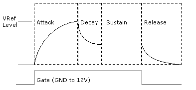
Gate and Multiple Triggers
Here we see that a trigger signal is applied along with the gate but that during the Decay cycle another trigger pulse is received. This causes a return to the Attack cycle at the voltage level that the envelope had decayed to.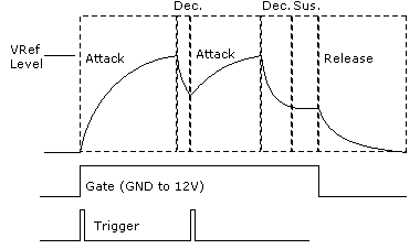
Gate Removed Prior to Sustain
Here the gate is removed before the voltage has decayed to the Sustain level. Subsequently the Release cycle is entered as soon as the gate is removed.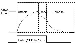
Long Attack and Gate Removed Prior to Decay Cycle
With a long Attack time the gate application and removal result in an AR (Attack-Release) type envelope.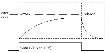
Trigger Only Applied
A trigger pulse without an accompanying gate will always result in a complete Attack cycle followed by a release cycle.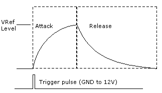
Retrigger Applied During Release
With triggers only applied the Release cycle can be interrupted by a trigger pulse and a new Attack cycle begun.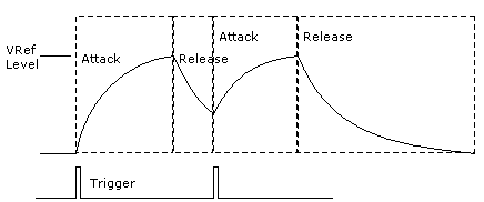
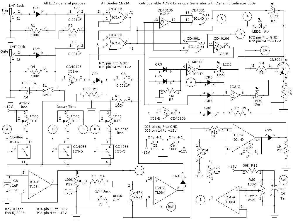
Retriggerable ADSR Envelope Generator With Dynamic State Indicator LEDs Schematic
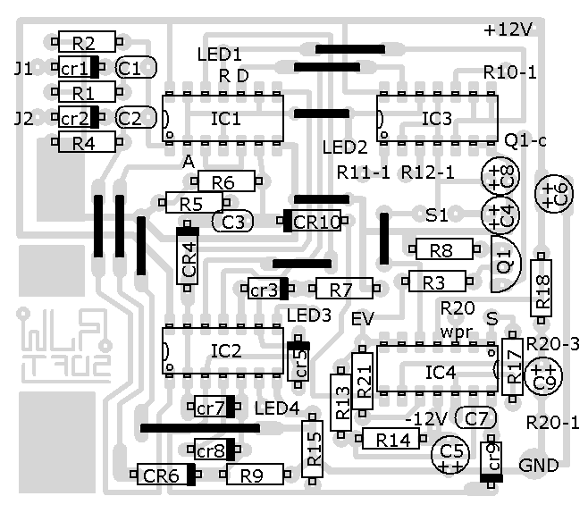
Retriggerable ADSR Envelope Generator With Dynamic State Indicator LEDs Parts Layout
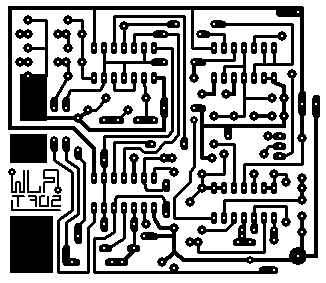
Retriggerable ADSR Envelope Generator With Dynamic State Indicator LEDs PCB Layout (Parts side View)
ADSR Envelope Generator Project Parts List
| Qty. | Description | Value | Designators |
|---|---|---|---|
| 5 | 1/4 Watt 1% Resistor(s) | 100K | R1, R4, R2, R5, R6 |
| 1 | 1/4 Watt 1% Resistor | 1K | R16 |
| 4 | 1/4 Watt 1% Resistor(s) | 1M | R15, R14, R7, R9 |
| 1 | 1/4 Watt 1% Resistor | 2K | R13 |
| 1 | 1/4 Watt 1% Resistor | 2M | R3 |
| 1 | 1/4 Watt 1% Resistor | 30K | R18 |
| 1 | 1/4 Watt 1% Resistor | 3K | R8 |
| 2 | 1/4 Watt 1% Resistor(s) | 47K | R21, R17 |
| 1 | CD4001 NOR Gate | CD4001 | IC1-A, IC1-B, IC1-D, IC1-C |
| 1 | CD40106 Hex Inverter | CD40106 | IC2-F, IC2-D, IC2-C, IC2-B, IC2-E, IC2-A |
| 1 | CD4066 Quad Analog SW | CD4066 | IC3-B, IC3-A, IC3-C |
| 3 | Ceramic Capacitor(s) | 0.001uF | C2, C3, C1 |
| 1 | Ceramic Capacitor | 10pF | C7 |
| 2 | Electrolytic Capacitor(s) | 10uF | C6, C5 |
| 1 | Electrolytic Capacitor | 15uF | C4 |
| 2 | Electrolytic Capacitor(s) | 1uF | C9, C8 |
| 4 | LED(s) | LED | LED4, LED1, LED3, LED2 |
| 1 | Operational Amplifier | TL084 | IC4-A, IC4-B, IC4-C, IC4-D |
| 3 | Phone Jack(s) | 1/4" Jack | J2, J1, J3 |
| 2 | Potentiometer(s) | 100K | R19, R20 |
| 3 | Potentiometer(s) | 1Meg | R12, R10, R11 |
| 1 | SPST Switch | SPST | S1 |
| 10 | Silicon Diode(s) | 1N914 | CR6, CR7, CR8, CR1, CR2, CR4, CR3, CR5, CR9, CR10 |
| 1 | Transistor NPN | 2N3904 | Q1 |