Ray Wilson authored this content while he was actively running MFOS as the founder and resident genius.
We retain the content because it reflects a valuable point of view representing that time and place.
Article by Ray Wilson
While recently building two units I discovered that modulation of the filter when using the integrated square wave from the LFO could be improved (deepened) by changing the value of R56 from 75K to 20K. This change permits more current to be delivered by the LFO when using the integrated square wave and permits C19 to charge and discharge more deeply during modulation. The parts list has been updated to include two (2) 20K resistors instead of one (1). Some customers may like the operation with the original 75K and others the 20K. You'll have the resistors for either response.
Features

|
|
IntroductionThe best way I can describe the MFOS "NOISE TOASTER" is this... "The MFOS NOISE TOASTER squeezes more fun out of a nine volt battery than you ever thought possible". This is an excellent project for anyone interested in synth-diy or "noise" boxes. You'll come back to it again and again due to it's portability, simplicity of operation and incredibly wide range of sound possibilities. Along the way you'll also learn a new circuit trick or two for use in your own hobby builds. Get ready to have a TON of creative, imaginative sound making fun.
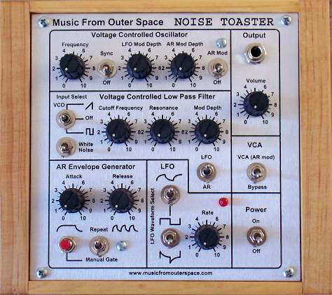
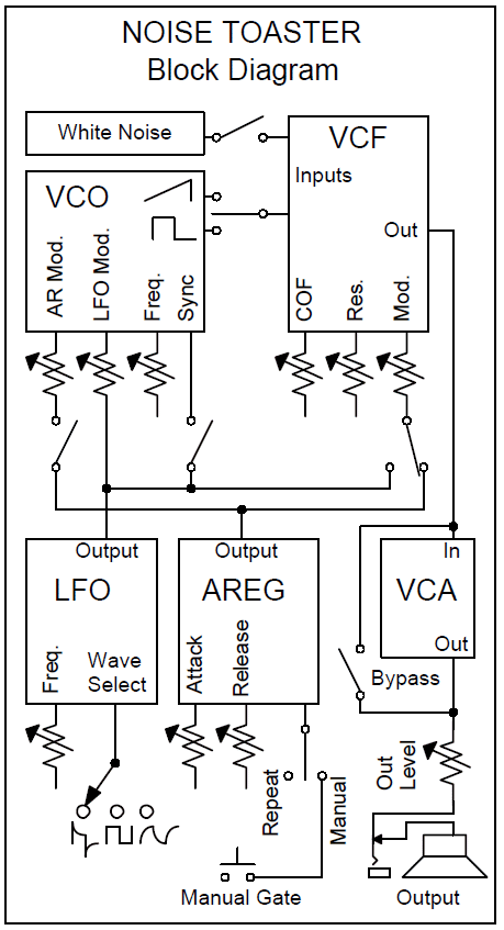
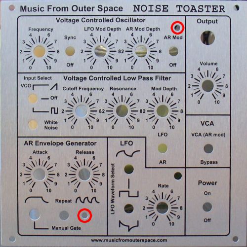
OverviewThe MFOS NOISE TOASTER circuit consists of seven main components: a voltage controlled oscillator (VCO), a white noise generator, a voltage controlled low pass filter (VCF), a low frequency oscillator (LFO), a simple AR envelope generator (AREG), a simple voltage controlled amplifier (VCA), and a one watt amplifier that drives a small speaker. The unit is powered by one nine volt battery and due to the low current drain of the LM324 (Lo-Power Quad Op Amp) it gets a lot of miles out of a nine volt battery. The circuit draws about 15mA to 25mA dependent on volume level when using the internal amp. When using line out the unit draws slightly under 15mA.
Sample MP3s (All recorded dry) |
Block Diagram
|

MFOS NOISE TOASTER Schematic Page 1
View as PDF Table of Contents
Voltage Controlled Oscillator (VCO)
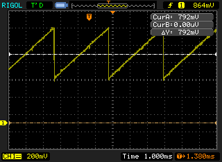
The voltage controlled oscillator (VCO) in the NOISE TOASTER provides a nice wide range of frequency and two waveforms (ramp and square). It is known as a ramp core design since the main waveform results in a ramp wave. In a modular synthesizer this wave would be converted into several other waveforms through various electronic techniques. In the NOISE TOASTER this wave is also converted to a square wave. IC U1-C (1/4 LM324 Low Power Quad Op Amp) is used to sum the control voltages that modulate the frequency of the VCO. Three sources of frequency modulation are applied to this op amp which is used as an inverting summer. Potentiometer R1 (100K linear pot) is used to control the frequency of the VCO. It's ends connect to BN and BP (Battery Negative and Battery Positive) thus the wiper sees from 0V (min setting) to 9V (max setting) which is applied via R2 (75K 1/4W resistor) to the inverting input of U1-C.
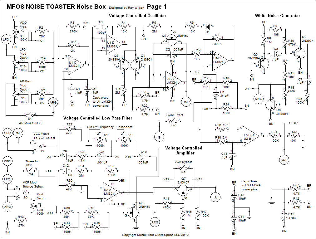
Potentiometer R13 (100K linear pot) is used to control the amount of LFO modulation applied to the summing inverter via R14 (100K 1/4W resistor) to the inverting input of U1-C. At minimum setting it applies BN to the summer and at maximum setting it applies the LFO output to the summer. Potentiometer R20 (100K linear pot) is used to control the amount of AR modulation applied to the summing inverter via R21 (36K 1/4W resistor) to the inverting input of U1-C. At minimum setting it applies the vco's virtual ground to the summer and at maximum setting it applies the AR Generator output to the summer. Switch S1 (SPST mini toggle) was added because even at minimum setting the AR generator was modulating the VCO ever so slightly but enough to drive you nuts if you didn't want it to. The summing resistors used (R2, R14 and R21) are different values because the amplitudes of the modulation sources vary. Even though the AR generator's output is lower in amplitude than the LFO's output by using the lower value summing resistor for it (R21 36K as opposed to R14 100K) we still get a wide range of modulation from the AR. Resistor R3 (270K 1/4W resistor) connects to R3 and biases the summing amp more toward BP to compensate for the fact that two of the VCO's modulation control pot's have one end tied to BN. The 2K feedback resistor between U1-C's output and inverting input sets it's gain quite low (the gain for each input varies due to each having a different value input resistor). However as an example, a 100K input resistor and a 2K feedback resistor result in a gain of 1/50th. This is done because the linear voltage to exponential current converter that follows only needs a very small change in voltage to change the frequency of the oscillator a great deal. As a matter of fact when the output of U1-C changes by about 18mV (up or down) the oscillator's frequency changes by approximately an octave (also up or down). The expo convertor is made up of U1-D and associated components C1, R4, Q3, Q4, and R16. Suffice it to say that the expo-convertor (as it is known) causes current to be "sinked" i.e consumed into the collector of Q4 in a very special ratio. As the voltage on the base of Q3 changes by approximately 18mV up or down the current into the collector of Q4 doubles or halves. As current sinks into the collector of Q4 it pulls current out of the inverting input of U1-A (pin 2) wired as an integrator. Capacitor C2 (.001uF ceramic cap) in the feedback loop helps you identify the fact that U1-A is being used as an integrator. This causes the voltage on the output of U1-A to ramp up at a rate that depends on the magnitude of the current sinked by Q4. When the voltage level at the output of U1-A goes slightly above U1-B's threshold voltage level which is set by voltage divider R17 (10K 1/4W resistor) to BP and R18 (15K 1/4W resistor) to BN U1-B's output goes rapidly from 0V to 9V. Resistor R7 (300K 1/4W resistor) provides U1-B used as a comparator with a slight bit of hysteresis. The high voltage from U1-B's output drives current through D1 (1N914 high speed switching diode) and R6 (10K 1/4W resistor) and turns on Q1 (2N5457 N-Channel JFET) which discharges C2 (U1-A's integrator cap) causing the output of U1-A to fall rapidly to the mid level voltage (virtual ground #1) which is set by resistors R23 (4.7K 1/4W resistor) to BP and R22 (4.7K 1/4W resistor) to BN. These two resistor set the virtual ground voltage level used by the VCO. Once Q1 causes the integrator cap (C2 .001uF ceramic capacitor) to discharge, U1-B's output goes to 0V again, shutting off Q1 and allowing U1-A's output to ramp up again. This cycle repeats resulting in a ramp waveform at the output of U1-A whose frequency is dependent on the current being sinked by Q4. As the voltage on the inputs to the summing inverter vary the frequency of the VCO varies over a very wide range.
To generate the square wave we feed the ramp wave to both the inverting and the non-inverting inputs of op-amp U2-B. The non-inverting input sees the raw ramp wave via 10K resistor R26. The inverting input sees the average voltage of the ramp wave due to the fact that we apply low pass filtering to it by using a 2M resistor (R30) to integrate the ramp wave onto C11 (.1uF ceramic cap). Even at low VCO frequencies R30 and C11 provide sufficient filtering to present the inverting input of U2-B with the average voltage of the ramp wave output of U1-A. U2-B is wired as a comparator (no feedback resistor) and thus when the ramp wave goes up it's instantaneous voltage presented to the non-inverting input of U2-B via 10K resistor R26 goes above the filtered average on the inverting input of U2-B (pin 6) and the output of U2-B shoots high rapidly (from 0V to 9V). When the ramp wave shoots low (Q1 turned on) it's instantaneous voltage presented to the non-inverting input of U2-B via 10K resistor R26 goes below the filtered average and the output of U2-B shoots rapidly low (from 9V to 0V). We use a voltage divider to attenuate the level of the square wave to make it compatible with the ramp wave prior to applying it to the input of the voltage controlled filter.
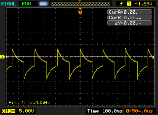
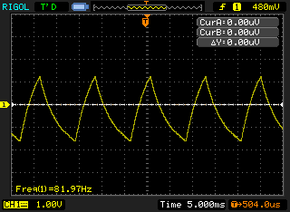
Images showing the ramp and square waves. Notice that the ramp sits on a bias level and oscillates above virtual ground #1 and the square wave oscillates about virtual ground #1. The scope ground was at U1-A pin 3.
| Ramp Wave (Circuit Point X3) Scope ground at U1-A pin 3 (virtual ground #1) | Square Wave (Circuit Point X7) Scope ground at U1-A pin 3 (virtual ground #1) |
 |
 |
When switch S2 is turned on we apply the square output of the Low Frequency Oscillator (LFO) to the junction of C6 (.01uF capacitor) and R24 (100K 1/4W resistor). The pulse that is conducted to the threshold bias of U1-B via C6 when the LFO's square wave goes up or down causes the integrator to be reset which results in producing an unusual waveform with harmonics of both the LFO and the VCO. The LFO must be at or near the top of it's frequency range to hear the effect.
Voltage Controlled Filter (VCF)
The voltage controlled filter (VCF) in the NOISE TOASTER is as simple as you can get and still provide useful functionality. It is a low pass "T" type filter (due to the two caps and resistor to ground in the feedback loop resembling a "T"). Feedback resistor R35 (4.7M 1/4W resistor) and the two filter capacitors C9 and C10 (both .001uF ceramic caps) determine the filter's characteristics and gain. The filter's cutoff frequency increases as we decrease the resistance between the junction of the two feedback capacitors and the circuit's virtual ground (this is done by R28 100K potentiometer). The filter's Q increases as we decrease the resistance between the two feedback caps of the filter (this is done by R29 100K potentiometer).
In order to permit the filter's cut off frequency to be controlled by a voltage we use Q8 (a 2N5457 N-Channel JFET) in it's voltage controlled resistor (VCR) mode. As we apply more positive voltage to the gate of Q8 the resistance between the drain and the source goes down resulting in the filter's cutoff frequency going up. We bias the voltage that is fed to Q8's gate so that it's drain to source resistance varies nicely as we apply the voltages from the unit's modulators (LFO and AR Generator).
Potentiometer R38 (100K linear pot) in conjunction with S6 (SPDT Center Off mini-toggle switch) is used to adjust the level of the LFO or ARG that is applied to the gate of Q8 and subsequently modulates the cut off frequency of the VCF. Resistors R39 (39K 1/4W resistor), R40 (39K 1/4W resistor), R44 (100K 1/4W resistor) and R45 (100K 1/4W resistor) both current limit and bias (to both BP and BN) the modulation sources to permit Q8 to work in its resistive region. When the modulation signals are increased via adjustment of R38 the transistor acts as a voltage controlled resistor and serves the same purpose as the cut off frequency pot (i.e. bringing the junction of C9 (.001uF ceramic capacitor) and C10 (.001uF ceramic capacitor) closer or further from ground. Resistor R43 (27K 1/4W resistor) is mounted on the front panel (see front panel wiring diagram) and limits the low side of the VCF Mod Depth pot.
The filter rings slightly even when the resonance control is at minimum but rings quite a bit more when the resonance (Q) control is turned up. Switches S3 (SPDT Center Off mini-toggle switch) and S4 (SPST mini-toggle switch) are used to apply the unit's VCO output and White noise to the inputs of the filter. The input signals are capacitively coupled (VCO via C8 and Noise via C12) to the input resistors (VCO via R33 and Noise via R34) and finally to the inverting input of the filter (U2-A pin 2). U2-A pin 3 is connected to virtual ground #2 in the unit (formed by 1/4W resistors R37 4.7K and R42 4.7K and 470uF filter cap C15). Resistors R27 and R36 (both 1/4W 47K) quiet the inputs to the filter when the switches, which apply the oscillator and/or noise, are open.
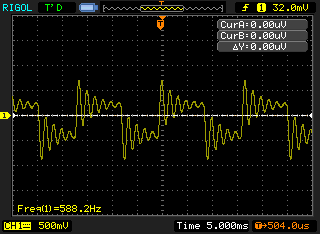
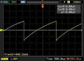
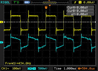
Images showing the ramp and square waves after filtering via the VCF Scope ground on circuit point marked GND (virtual ground #2). Cutoff frequency set to 8 and Resonance set to 10. Signal operates about virtual ground #2.
| Square wave through VCF high resonance. | Ramp wave through VCF high resonance (VCF inverts the ramp to a sawtooth). |
 |
 |
Voltage Controlled Amplifier (VCA)
I said it was simple and it really is. This VCA is LO-FI in that it distorts the signal going through it a bit (flattening the wave a bit on one side) but it still passes the signal faithfully enough that it provides some interesting effects. The VCA is a single 2N5457 N-Channel JFET used in the VCR (voltage controlled resistor) mode. We apply the output of the VCF to Q7's Drain and take the output from it's Source which is also connected to BN via load resistor R47 (100K 1/4W resistor). As voltage on the gate is made more positive by the output of the AR Generator the resistance between the Drain and Source goes down thus dropping the signal from the input (Q7's Drain) onto R47. Q7's Source (the VCA's output) is applied to the top of the unit's volume pot R66 (100K linear taoer potentiometer). Switch S5 (SPST) is used to bypass the VCA by simply shorting the Drain and Source of Q7.
White Noise Generator
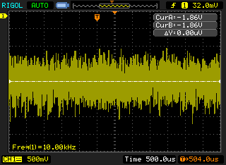
The NOISE TOASTER's White Noise Generator is, not surprisingly, based on the emitter base breakdown of an NPN transistor. Q5 (2N3904 NPN Transistor) is used as the noise source. BP is applied to Q5's emitter via current limiting resistor R8 (1M 1/4W resistor). Since the EB breakdown voltage of the 2N3904 is around 5 volts the junction breaks down resulting in white noise being produced at the R8, Q5-Emitter junction. The noise is then capacitively coupled into a two stage discrete transistor amplifier made up of Q2, Q6 and associated components. The first stage is made up of C3 (.1uF ceramic ac coupling capacitor), R9 (10K 1/4W resistor) load resistor, R10 (470K 1/4W resistor) collector base feedback biasing resistor and Q2 (amplifier). The transistor amplifies the signal applied to it's base and supplies the amplified signal via the junction of Q2's collector, R9, and R10. The second stage is obviously just a repeat of the first stage and simply supplies some more gain. This arrangement results in a nice clean noise that I was able to get from just about any 2N3904 I picked from my parts drawer for Q5. However you may need to test a few before finding a nice noisey one. When your battery starts to run down the first thing you'll notice is that the noise will stop working once the voltage is too low to exceed the emitter base breakdown voltage of Q5.
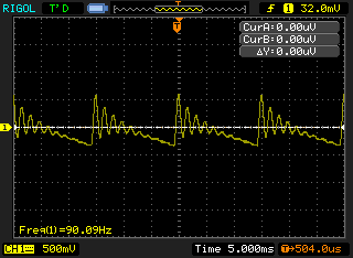
| Noise at circuit point X4. | Noise through VCF. Cutoff = 10 Resonance = 0. |
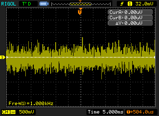 |
 |
MFOS NOISE TOASTER Schematic Page 2
View as PDF Table of Contents
Power Supply
Battery B1 is switched into the circuit by S11 (SPST toggle switch). Capacitor C23 (470 uF) is the main supply filtering cap. It holds a good bit of charge which supplements the battery when the unit draws additional current. There are two virtual ground points in the circuit because during breadboarding the only way I could reduce interaction among what we'll call the unit's "micro-modules" was to do so. This is the first one. Resistors R22 and R23 (4.7K resistors) form a voltage divider that supplies a voltage level which is halfway between the battery's plus and minus terminals. This voltage is used as a ground reference in part of the circuitry. C4 and C5 (.1uF ceramic capacitors) are placed very close to the power pins of IC1 (LM324) to stabilize it's operation and filter power supply transisent noise from polluting the op amp's bias network. The second is this. Resistors R37 and R42 (4.7K resistors) form a voltage divider that supplies a voltage level which is halfway between the battery's plus and minus terminals. This voltage is used as a ground reference in the other part of the circuitry. C15 provides the capacitive inertia to hold the mid-level where we want it. Capacitors C13 and C14 (10uF aluminum electrolytic caps) further filter the "two" voltages which are formed about the virtual ground (+4.5 and -4.5) and are placed close to the power pins of IC2 (LM324) to stabilize it's operation.
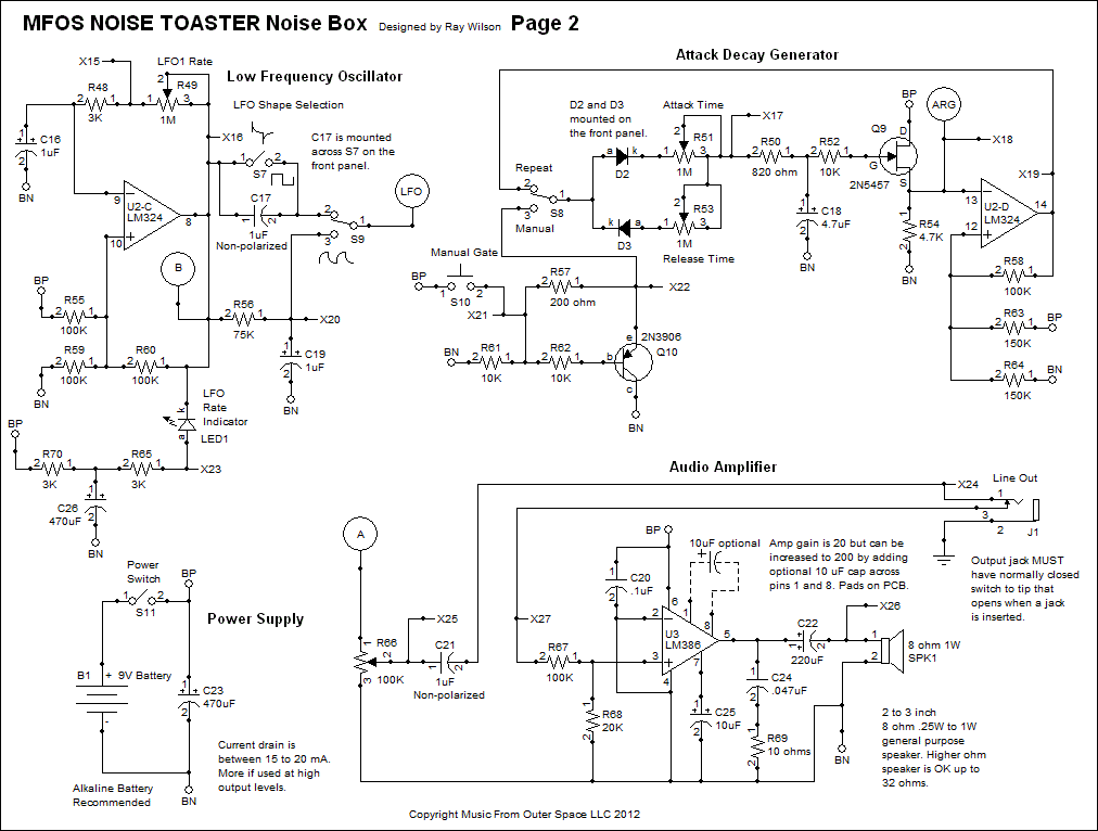
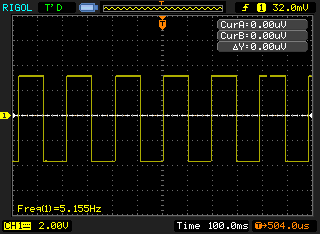
Low Frequency Oscillator (LFO)
We use a single op amp oscillator for the LFO. The frequency is determined by C16 (1uF electrolytic cap), R48 (3K 1/4W resistor), and LFO Rate potentiometer R49 (1M linear pot). The frequency range is about 2Hz. to about 247Hz. This circuit works as follows. Capacitor C16 is constantly being either charged or discharged by the op amp's output (via R48 and R49). If the op amp's output is high (just about at BP) the cap is being charged toward BP. At the same time the op amp's output is fed back to it's non-inverting input via R60 (100K 1/4W resistor) which changes the bias on that input. Without R60's contribution R55 and R59 (both 100K 1/4W resistors) would hold the non-inverting input at half the battery voltage. But R60 tips the voltage more positive or more negative depending on the output of U2-C. So if the output of U2-C is high the bias on the non-inverting input is about 5.5V to 6V. Capacitor C16 remember had previously been charging toward BN (because U2-C's output was low) so the voltage on it has to rise from below ground before finally getting above the voltage on the non-inverting input. When it does the output of U2-C shoots low and changes the bias on the non-inverting input to about 3.5 to 3V and C16 starts to discharge toward BN. When the voltage on C16 gets below the voltage on U2-C's non-inverting input the output of U2-C shoots high and the cycle continues resulting in square wave oscillation at the output of U2-C.
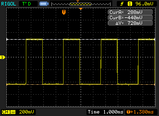
In order to provide additional interesting modulation wave shapes we modify the square wave to produce an integrated square wave using R56 (75K 1/4W resistor) and C19 (1uF electrolytic cap) and a differentiated square wave using C17 (1uF bipolar (non-polarized) aluminum cap). C17 is mounted on the terminals of S7 (SPST mini-toggle switch) on the front panel (see front panel wiring diagram). Switches S7 and S9 provide LFO waveform selection. Switch S7 selects either square (S7 on) of differentiated square (S7 off) and S9 selects between either one of those waveforms or the integrated square wave. The circled circuit point LFO is connected to the modulation level pots on the front panel (see front panel wiring diagram).
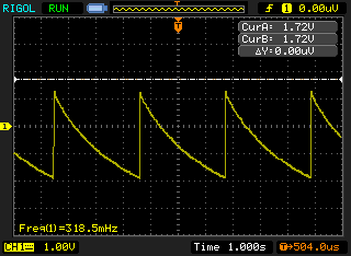
Images of the LFO output taken from the common pole of S9.
| LFO Square Wave. LFO Rate at 8 | LFO Integrated Square Wave. LFO Rate at 8 | LFO Differentiated Square Wave. LFO Rate at 8 |
 |
 |
 |
Attack Release Envelope Generator (EG)
The Attack Release Envelope Generator is again a very simple but effective implementation. In manual mode (S8 SPDT set to Manual) we use S10 (SPST N.O. Pushbutton) to apply a "gate" to the AR envelope generator. With pushbutton S10 open (not pressed) Q10 (2N3906 PNP transistor) is held in the on state (current can flow between the collector and the emitter) by R61 and R62 (both 10K 1/4W resistors) which connect Q10's base to BN (Battery Negative). In this condition Q10 discharges C18 (4.7uF electrolytic cap) via forward biased D3 (1N914 diode) and R53 (1M linear Release Time pot). When S10 is pressed BP (Battery Positive) is dropped on R61 (10K 1/4W resistor) and applied to the base of Q10 via resistor R62 (10K 1/4W resistor). This turns off Q10 and allows BP (Battery Positive) to be applied via R57 (200 ohm 1/4W resistor) to forward biased D2 and charges C18 via R51 (1M linear pot) Attack Time pot. When S10 is released again, C18 discharges via R53 and D3 through the now turned on Q10's collector to emitter. The attack and decay times are adjustable via pots R51 and R53 respectively. The voltage on C18 is buffered by Q9 (2N5457 N-Channel JFET). R52 applies the voltage from C18 to the gate of Q9 used in the source follower mode. The gate of Q9 is high impedance so the envelope voltage generated on C18 does not discharge through Q9's gate. The output of the AR generator occurs at the junction of R54 (4.7K 1/4W resistor) and the source of Q9 and is a lower impedance source of voltage with which we can supply the VCO and VCF modulation pots.
In "Repeat" mode (S8 set to Repeat) the output of U2-D which is wired as an inverting comparator is fed back to the gate input of the AR generator (junction of the anode of D2 and the kathode of D3). The three resistors that control the comparator's threshold level R58 (100K 1/4W resistor), R63 (150K 1/4W resistor), and R64 (150K 1/4W resistor) work in a manner that is similar to the LFO's comparator. As long as the voltage presented to U2-D's inverting input is below the level of the threshold voltage the output of U2-D is high (very close to BP) so C18 charges through D2 and R51 until the voltage exceeds the threshold voltage and then the output of U2-D shoots low. Now C18 discharges (via 1M Release Time pot R53 and D3) until the Q9 buffered voltage on the inverting input of U2-D goes lower than the threshold voltage and then U2-D's output shoots high. This cycle continues resulting in an oscillatory wave at point ARG whose rise time is controlled by the Attack Time pot (R51) and whose fall time is controlled by the Release Time pot (R53).
The circled circuit point ARG (X18) is connected to the modulation level pots on the front panel (see front panel wiring diagram).
Images of the AR output taken from circuit point X18.
| AR Output (X18) Attack Time = 0, Release Time = 0. | AR Output (X18) Attack Time = 5, Release Time = 0. | AR Output (X18) Attack Time = 0, Release Time = 5. |
 |
 |
 |
One Watt Audio Amplifier
Finally we have our amplifier which is basically U3 an LM386N-4 1W integrated audio amplifier. We add the components that the LM386N data sheet tells us to and voila we have a complete 1W amplifier. For more on the operation and internal circuitry of the LM386N see it's data sheet (Google LM386 and you'll find a plethora of them). The output of the simple JFET VCA is fed to one end of R66 which is used as a variable attenuator (volume pot) with the other side connected to battery negative.
We block DC from getting to the input of the amplifier via C21 (1uF bipolar (non-polarized) aluminum cap). As we advance R66 we pick off more and more VCA output and if we go the other way... less and less. Resistors R67 (100K) and R68 (20K) further attenuate the level fed to the amplifier's input from the volume pot so that we don't overdrive the amplifier resulting in distortion.
The line out jack's tip terminal is fed from AC coupling cap C21 (1uF bipolar aluminum cap) which connects to the 100K volume pot's (R66) wiper. The input to the LM386 amplifier (point X27) connects to the switch leg of the 1/4" jack. When no phone jack is inserted into J1 the switch leg contacts the tip tong and the internal amplifier is fed the AC coupled signal from the wiper of R66. When a jack is inserted into J1 the tip tong is forced away from the switch leg and the signal is no longer fed to the internal amplifier's input. The unit draws lowest current (approximately 15mA) when using line out.
Images of the Audio Amp Input (yellow - X27) and Output (blue - X26).
| Yellow is circuit point X27. Blue is circuit point X26. This is just to show that the output to the speaker should bear some resemblance to the signal fed into the amplifier. |
 |
Well that's that. Build it, connect the battery and turn the knobs and have fun making cool sounds. Put the output through effects for some extra craziness (echo, phase shifting, flanging, reverb, etc). Print out a few front panel templates to use as "patch" sheets to help you remember where to set the controls to recreate a unique sound later. Conserve sheets by using a separate color to denote each of several patches. Now go forth and toast some noise!
PC Board Designators
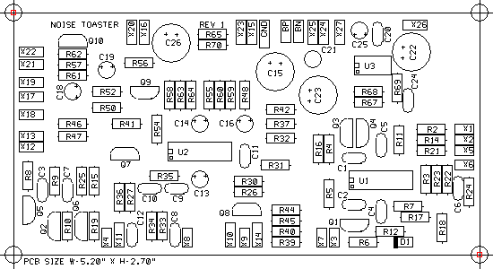
Table of ContentsThis view is good for when you are trouble shooting. Notice the pad next to X26. It is so you can connect the two speaker wires right there. The extra unmarked pad goes to BN (battery negative).
- R43 (27K 1/4W 5% resistor)
- D2 (1N914 diode)
- D3 (1N914 diode)
- C17 (1uF non-polarized aluminum capacitor)
- LED1 (General purpose LED)
PC Board Values
This view is good for when you are stuffing the PC board. Notice the pad next to X26. It is so you can connect the two speaker wires right there. The extra unmarked pad goes to BN (battery negative).
- R43 (27K 1/4W 5% resistor)
- D2 (1N914 diode)
- D3 (1N914 diode)
- C17 (1uF non-polarized aluminum capacitor)
- LED1 (General purpose LED)
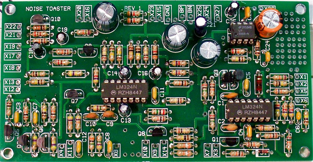
Populated PC Board
PC Board populated with components.
- R43 (27K 1/4W 5% resistor)
- D2 (1N914 diode)
- D3 (1N914 diode)
- C17 (1uF non-polarized aluminum capacitor)
- LED1 (General purpose LED)
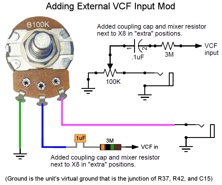
Modification Pads #1
Table of ContentsA question that always comes up with lo-fi units is. Can I put my own signal through the noise toaster's VCF and VCA? Why yes you can! These pads provide room for another coupling cap and mixing resistor for the VCF's input. If you're putting a low level signal through the unit (electric guitar) I suggest using .1uF for C and 1M for R. If you need more gain use a lower value resistor. For higher level signals I would go with .1uF for C and 4.7M for R. You can adjust the value of R to get as much signal as possible into the mix without distortion. Run a wire from the circled pad to the tip connector of a jack if you want to add an external input. Ground the added jack's ring to the units GND. You could add a 100K level adjustment pot between the jack and the pad for added flexibility. Connect the jack's tip terminal to one end of the pot's resistive element. Connected the other side of the pot's resistive element to GND. Connect the pot's wiper to the circled PCB pad. If using a pot use a 470K resistor for R since you will be able to attenuate higher level signals and have more gain for low level signals. Be sure and connect the correct end of the pot's resistive element to the jack's tip terminal so your level control has proper rotational response.
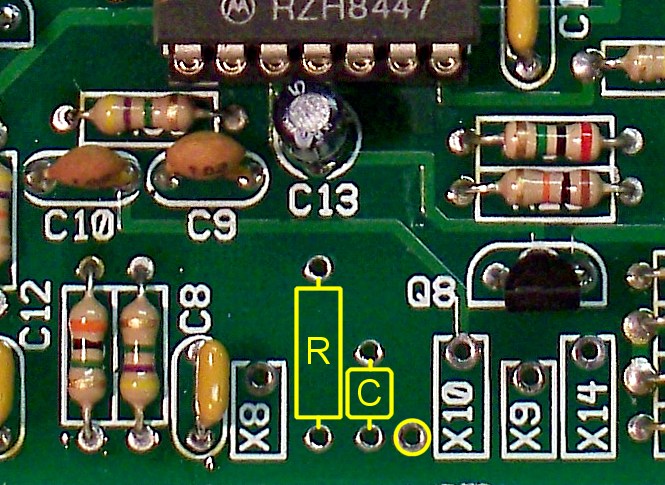
I show a 3M resistor because the filter is pretty high gain but you could reduce the value (2M, 1M, etc.) if the signal you are putting into the filter is too low in amplitude. And of course you could increase it if the signal you are putting into the filter is too high in amplitude.
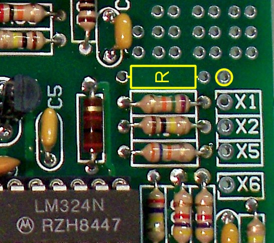
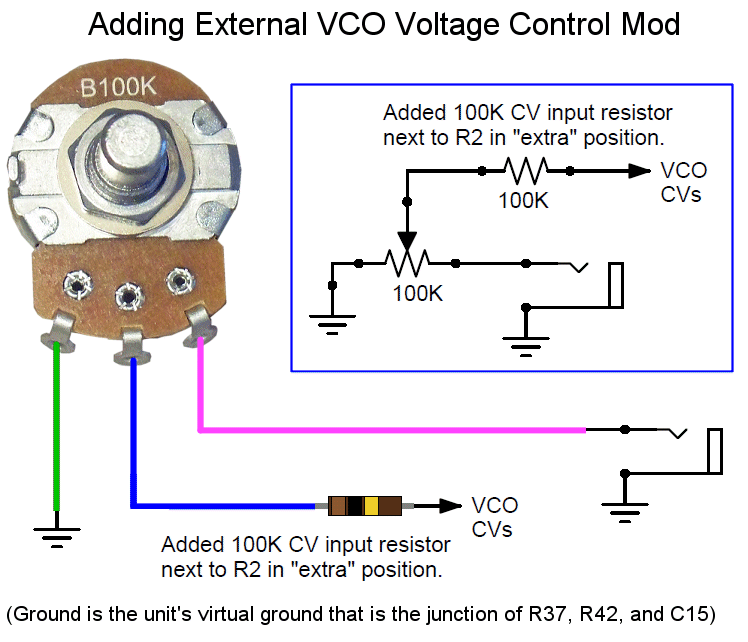
Modification Pads #2
Question number 2 is usually can I control the VCO with an external signal. Certainly you can! These pads are to add another CV input to the VCO. I would start with a value of 100K for R and then if you want more modulation from the source signal you could lower the value a bit (I would not go lower than about 47K). Run a wire from the circled pad to the tip connector of a jack if you want to add an external modulation input. Ground the added jack's ring to the units GND. As with the other modificaton you could add a pot to permit adjustment of the modulation.
Amplifier Gain Boost Option
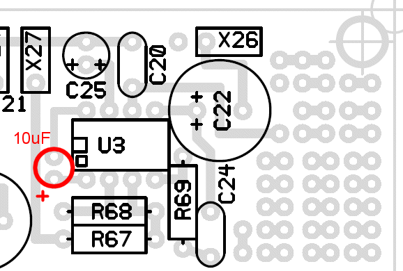
You have the option to change the gain of the amplifier from it's normal 20 to an ear splitting 200 by adding a 10uF electrolytic capacitor between pins 1 and 8 of U3 ( LM386N-4 One Watt Amplifier chip). Be sure to observe the polarity of the cap if you use it (positive side to goes to pin 1). There is no legend on the board for this component but I did put two pads on the PC board in case you want to use it. (see the image below). Adding the gain increasing cap causes the amplifier to draw a lot more current (about 5X more) which will eat your battery faster than you can say "DEAD BATTERY" so if you use it buy some Duracell stock first. Additionally if using the gain boosting cap I recommend you use a speaker rated for 1W since you may burn out a lower power speaker coil.
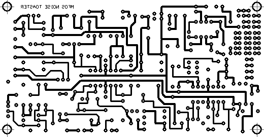
PC Board Bottom Copper
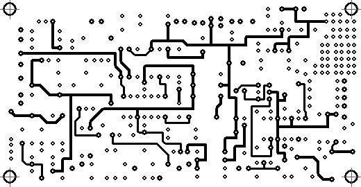
PC Board Top Copper
PC Board Silk Screen
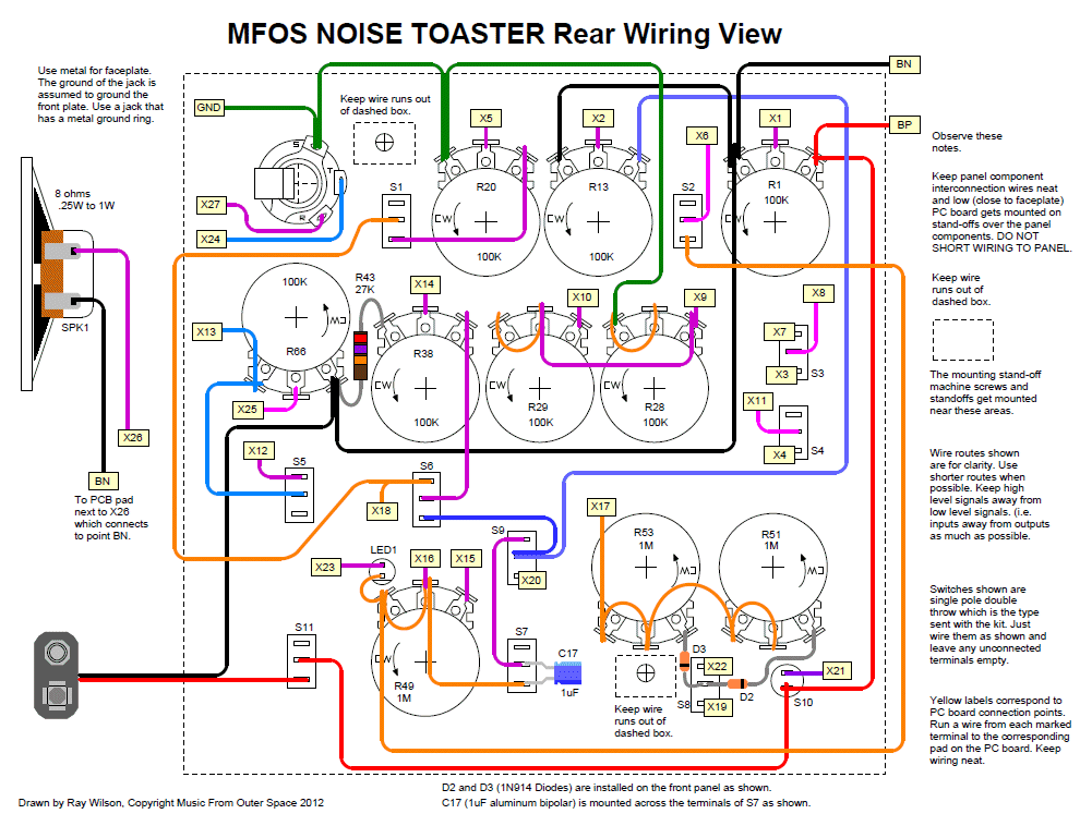
Front Panel Wiring
View as PDF Table of Contents
- R43 (27K 1/4W 5% resistor)
- D2 (1N914 diode)
- D3 (1N914 diode)
- C17 (1uF non-polarized aluminum capacitor)
- LED1 (General purpose LED)
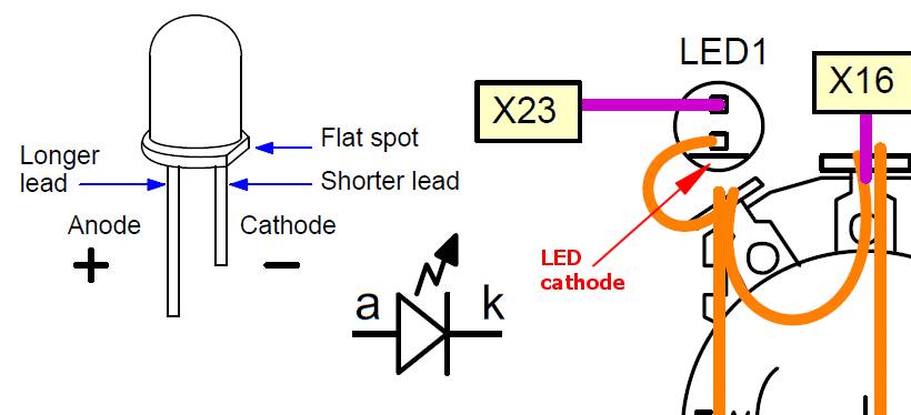
LED Orientation
The LED shown in the panel wiring has a line marking the LED's cathode lead. LEDs have two things to help identify which lead is which. The flat spot on the physical LED identifies the cathode lead. On new LEDs (not removed from equipment) the anode lead is longer than the cathode lead.
All 1/4" jacks are not created equal. The solder lugs may not always be arranged as shown in the following diagram so it is important to "ring out" your jack to confirm which lug goes to which jack component. "Ring out" means to use your ohm meter to read the resistance between the jack's components - tip prong, ground sleeve and switch leg and its solder lugs. Since this is a "switched jack" you need to remember that the switch lug is connected to the tip lug when no phone plug is inserted. Slip a piece of paper in between the jack's tip prong and its switch leg so you can tell them apart when you measure the resistance between the solder lugs and the jack components - tip prong, ground sleeve and switch leg. Your meter should be set to the lowest ohm setting. When you measure connectivity between two points the meter should read the same as when you touch its leads together.
Once you're certain of which lug connects to which corresponding jack component:
- Connect the tip lug to point: X24
- Connect the ground-sleeve lug to point: GND
- Connect the switch-leg lug to point: X27
This is just a suggestion but if you make your own unique panel make a corresponding wiring diagram to avoid panel wiring mistakes. They can be bears to trouble-shoot.
IMPORTANT!!! - THIS VIEW IS LOOKING AT THE MOUNTED PANEL CONTROLS FROM THE REAR OF THE PANEL.
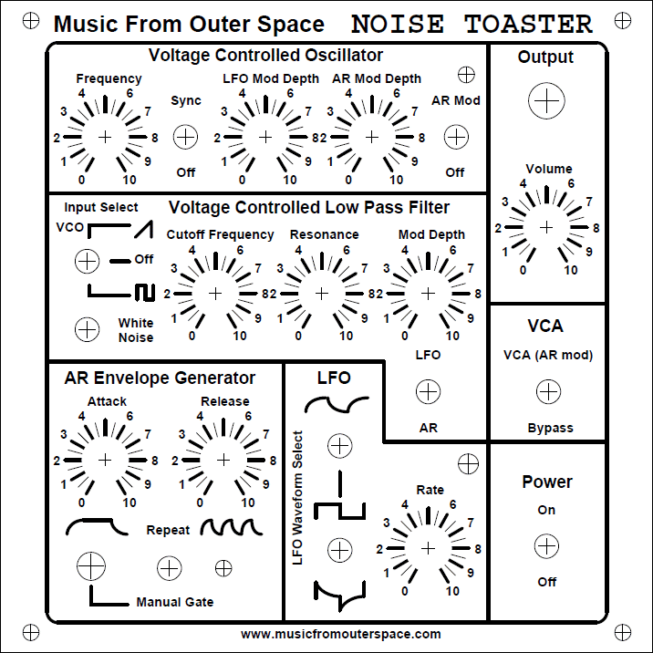
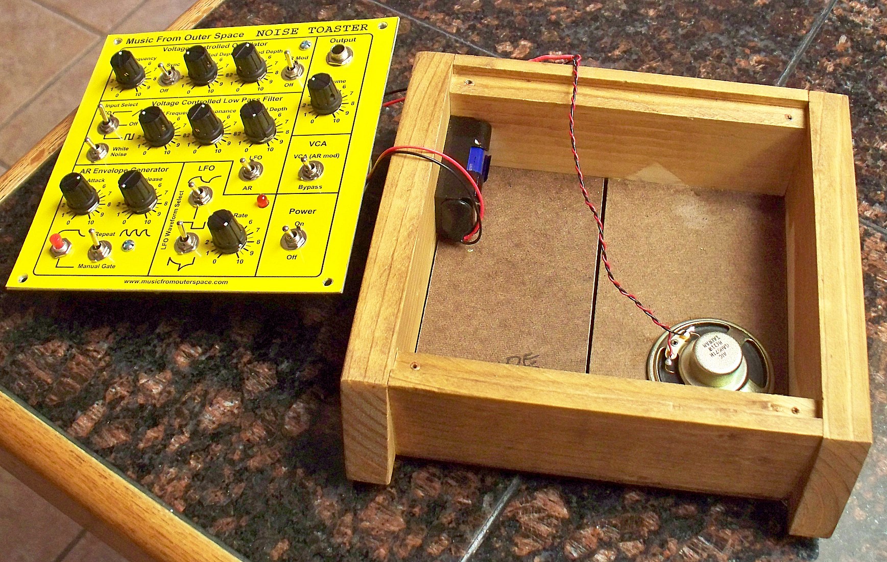
Front Panel Template
View as PDFThe PDF should print in actual size. Don't apply any scaling or page filling options. To use this image you need to scale it when printing so that it prints as 6.5" x 6.5". The two 5/32" diameter holes (one under the AR generator Repeat symbol and one above the VCO "AR Mod" title) are used to mount the PC board on standoffs with 1.25" long 6-32 machine screws and nuts. This image can also be used as a "patch sheet" to help you remember the settings for the various amazing and unusual sounds you discover.
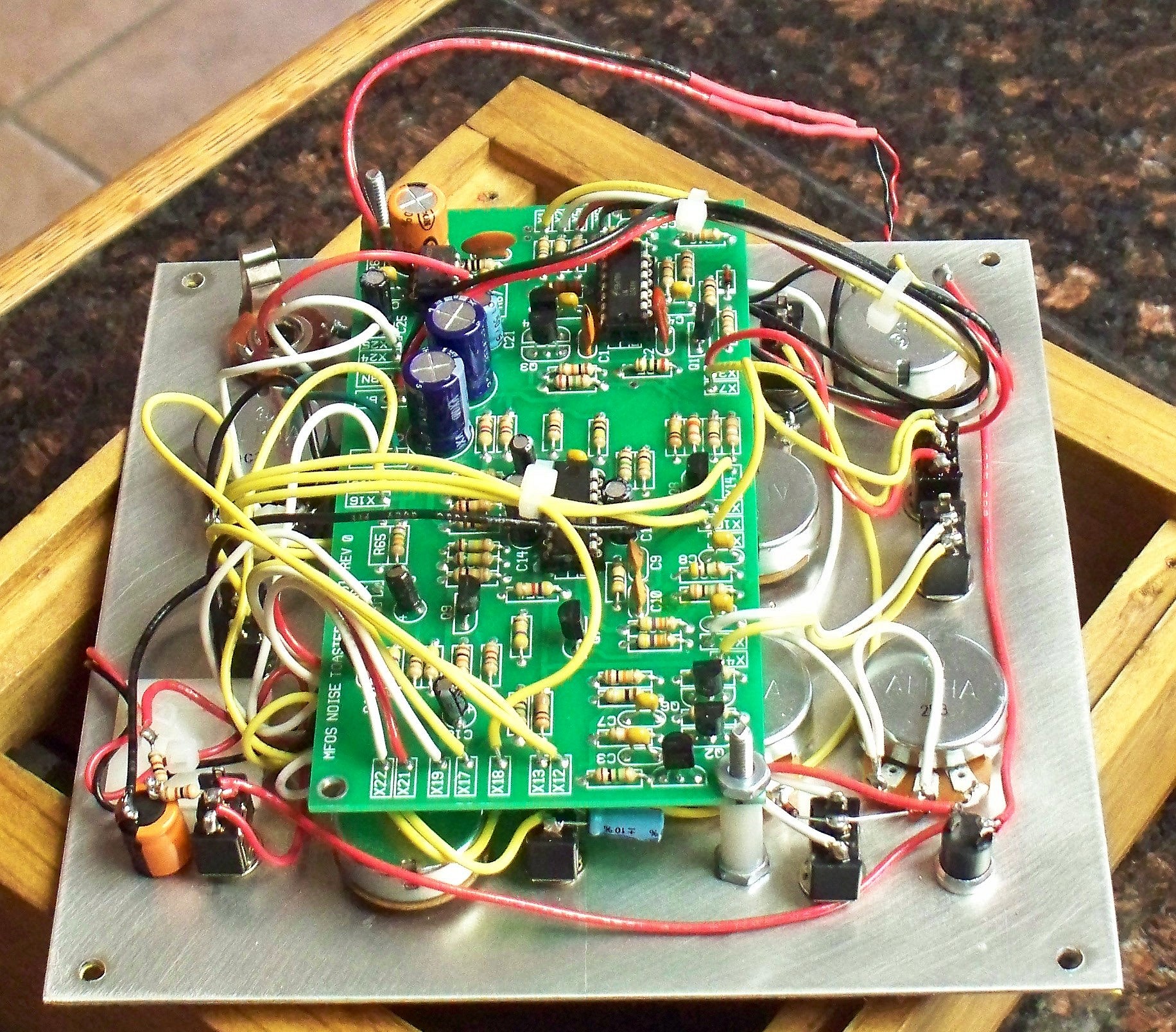
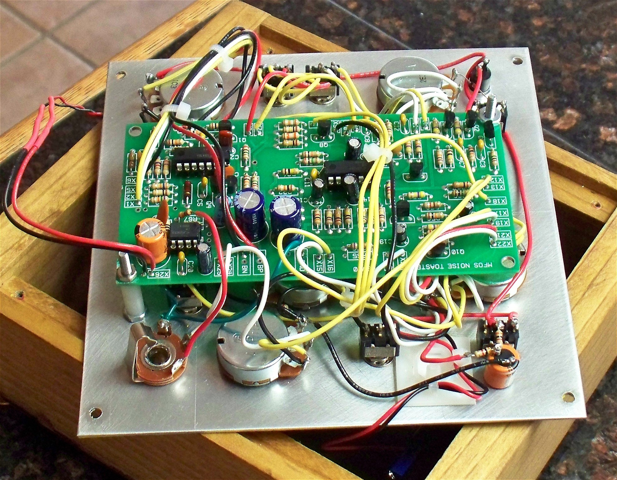
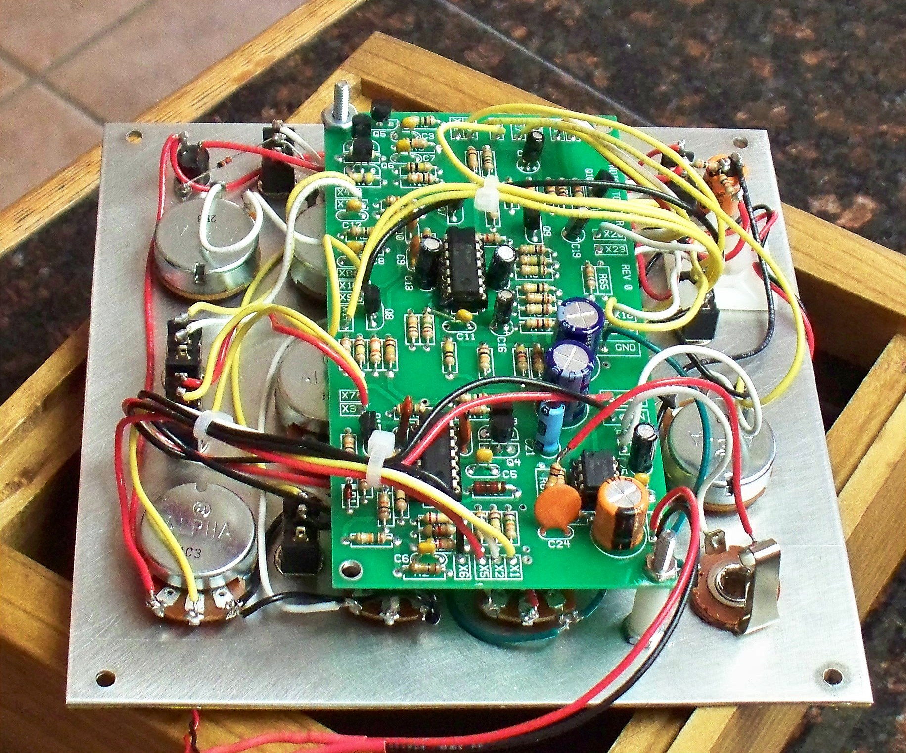
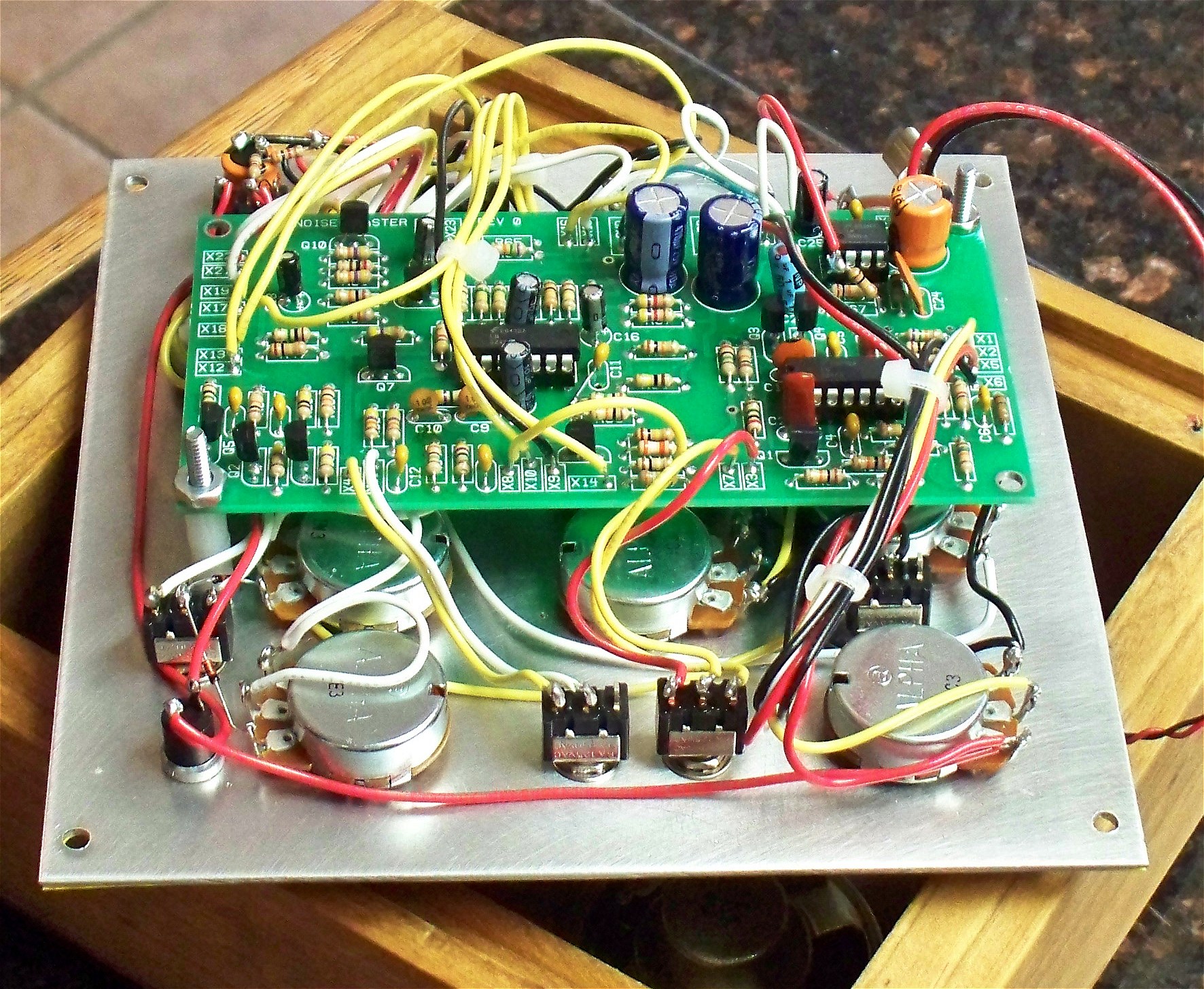
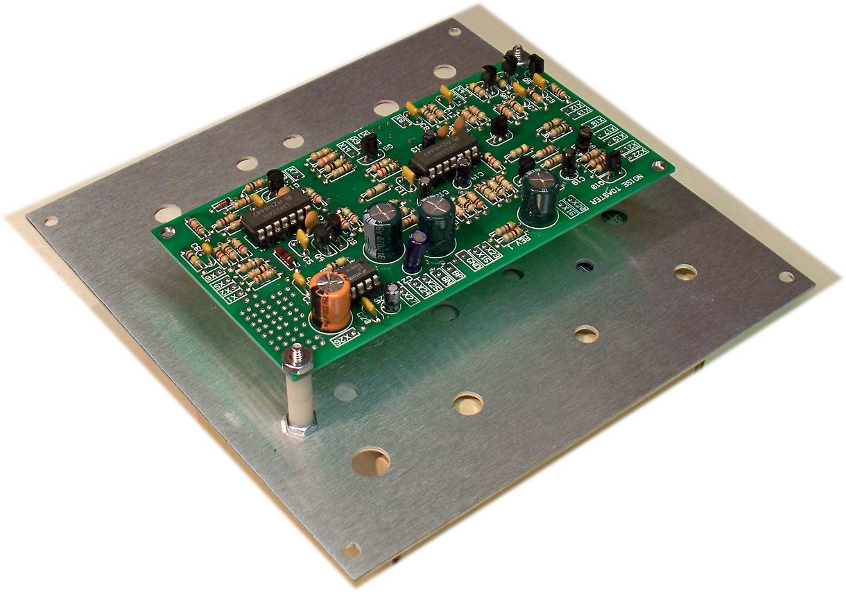
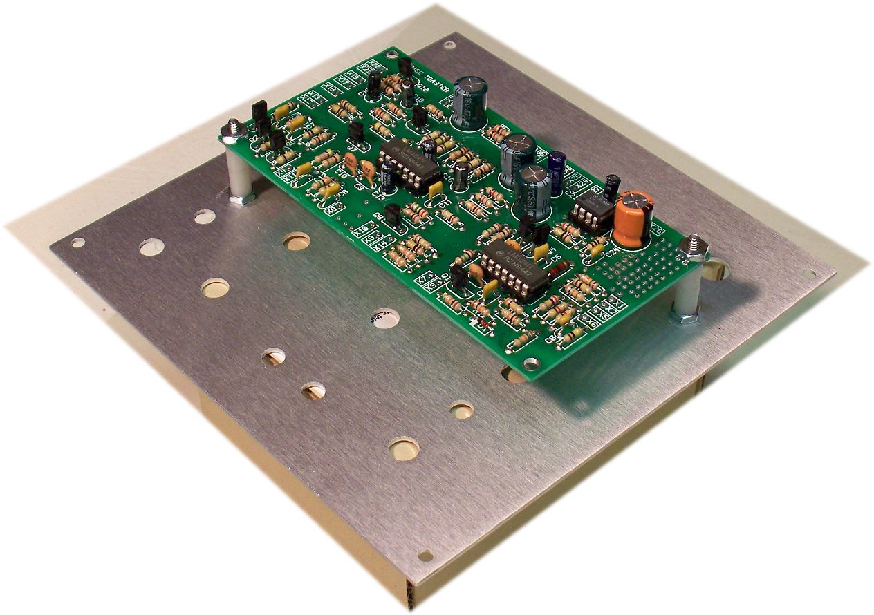
Pictures From the Prototype Build
NOTE! This is the prototype PC board so there will be some minor differences between this and the production PC boards but the main idea of how to mount the PC board and the idea behind wiring the panel components to the PC board is clearly demonstrated. The components (resistors and capacitor) near the power switch and the fact that a wire goes to one end of a resistor that has been disconnected from the PC board have both been resolved on the production PC boards.
I mounted my speaker on the bottom of the case. I would recommend some screen or grill cloth to prevent curious fingers from poking a hole in your speaker. The battery holder can be mounted on either the inside or the outside of the case. Sometimes it's easier to just have it on the outside so you don't have to open and close the case every time you change it.
I mounted the PC board to the front panel by using 1.5" long 6-32 machine screws and and 2 nylon standoffs for each screw. Each nylon standoff is 1/4" in diameter and 3/8" long (2 are 6/8" long). I used two of them in opposite corners of the PC board (all four corners would have been overkill IMHO) where I found some space among the front panel controls where the screw heads wouldn't be too obtrusive. The board is mounted so that the soldered side hovers above the panel components and the component side is accessible from the back of the panel (this arrangement makes for easy trouble shooting). However, it makes getting at the wires under the board difficult so I suggest you don't connect the PC board to the panel until you are certain the wiring under it is 100% correct. You may also need to remove the PC board during trouble shooting so to repeat don't secure the PC board with the machine nuts until you know the board and panel are properly interconnected and the circuit works as expected.
I first mount the panel components to the front panel as shown in the panel wiring diagram including any panel mounted electronic components (see the highlighted text near the PC board component placement image). Next I run the panel mounted component interconnection wires, making sure not to solder component terminals that will also host a wire that runs to the PC board until I add those wires later. Lastly I add the wires that will run to the PC board one at a time. I do this by eyeballing how much wire each run from the panel to the PC board will require (leave sufficient slack to be able to remove the PC board to trouble shoot later if necessary) and then cutting it to length. I then strip insulation from the wire's ends and add a label to the end that will eventually be soldered to the PC board. For wire labels I use the larger colored dots available at office supply stores and mark the appropriate "X" designator on it. After that I solder the one end to the appropriate place on the front panel. When all of the wires that will run to the PC board are measured, marked and soldered to the front panel I mount the PC board loosely to the panel. Next I remove the label and solder the marked wires from the panel to the appropriate pad on the PC board one at a time. I solder the wires to the top side of the PC board. The plated-through vias make this no more difficult than soldering from the bottom copper side. Leave a 1/16" inch or so of stripped wire above the pad and carefully apply the soldering iron tip to the top pad and stripped wire simultaneously while feeding in a small amount of thin solder. Avoid applying too much solder or applying the soldering iron to the wire's plastic insulation. When you see the solder flow and you've added an 1/8" to a 1/4" of thin solder to the joint it is complete. Don't shake the wire during soldering or the solder won't solidify properly and you may get a "cold solder joint" (gray and crusty looking). If a joint looks "cold" apply a wee bit more fresh solder so that the joint looks shiney. An excellent tool to help stabilize the wires while soldering is known as a "Helping Hands". It's a Rube Goldberg looking thing with a weighted base and adjustable arms with alligator clips you can buy at Radio Shack or similar type store (and of course on-line) that you use to position items you want to solder together.
 |
 |
 |
 |
 |
MFOS NOISE TOASTER Noise Box Parts List
Table of Contents
All integrated circuits need to be DIP packages. When shopping for chips remember that the numbers will have suffixes like BE or BC but as long as they are DIP packages you will be fine. The suffixes typically indicate temperature ranges and package materials (plastic, ceramic, etc).
MFOS sells a pack of 5 brand new Fairchild 2N5457 N-Channel JFET
Capacitors should be rated for 16V or better.
| Qty. | Description | Value | Designators |
|---|---|---|---|
| 2 | LM324 Quad Low Power Op Amp | LM324 | U1, U2 |
| 1 | LM386N4 (or N3) Low Voltage Audio Power Amp | LM386 | U3 |
| 1 | 2N3906 | 2N3906 | Q10 |
| 4 | 2N5457 N Channel JFET | 2N5457 | Q1, Q7, Q8, Q9 |
| 5 | Transistor NPN 2N3904 | 2N3904 | Q2, Q3, Q4, Q5, Q6 |
| 3 | 1N914 High Speed Sw. Diode | 1N914 | D1, D2, D3 |
| 1 | General Purpose Red LED | LED | LED1 |
| 7 | Linear Taper Potentiometer | 100K | R1, R13, R20, R28, R29, R38, R66 |
| 3 | Linear Taper Potentiometer | 1M | R49, R51, R53 |
| 3 | Resistor 1/4 Watt 5% | 2M | R5, R16, R30 |
| 1 | Resistor 1/4 Watt 5% | 300K | R7 |
| 1 | Resistor 1/4 Watt 5% | 36K | R21 |
| 1 | Resistor 1/4 Watt 5% | 15K | R18 |
| 2 | Resistor 1/4 Watt 5% | 39K | R39, R40 |
| 3 | Resistor 1/4 Watt 5% | 3K | R48, R65, R70 |
| 5 | Resistor 1/4 Watt 5% | 4.7K | R22, R23, R37, R42, R54 |
| 2 | Resistor 1/4 Watt 5% | 4.7M | R33, R35 |
| 3 | Resistor 1/4 Watt 5% | 470K | R10, R19, R41 |
| 2 | Resistor 1/4 Watt 5% | 47K | R27, R36 |
| 2 | Resistor 1/4 Watt 5% | 75K | R2, R56 |
| 1 | Resistor 1/4 Watt 5% | 820 ohm | R50 |
| 1 | Resistor 1/4 Watt 5% | 10 ohms | R69 |
| 12 | Resistor 1/4 Watt 5% | 100K | R14, R24, R25, R31, R44, R45, R47, R55, R58, R59, R60, R67 |
| 11 | Resistor 1/4 Watt 5% | 10K | R4, R6, R9, R12, R15, R17, R26, R32, R52, R61, R62 |
| 2 | Resistor 1/4 Watt 5% | 150K | R63, R64 |
| 1 | Resistor 1/4 Watt 5% | 3M | R34 |
| 2 | Resistor 1/4 Watt 5% | 1M | R8, R46 |
| 1 | Resistor 1/4 Watt 5% | 200 ohm | R57 |
| 2 | Resistor 1/4 Watt 5% | 20K | R68, Extra for optional R56 replacement. |
| 1 | Resistor 1/4 Watt 5% | 270K | R3 |
| 1 | Resistor 1/4 Watt 5% | 27K | R43 |
| 1 | Resistor 1/4 Watt 5% | 2K | R11 |
| 2 | Capacitor Aluminum Bipolar (non polarized) | 1uF | C17, C21 |
| 3 | Capacitor Ceramic | .001uF | C2, C9, C10 |
| 1 | Capacitor Ceramic | .047uF | C24 |
| 8 | Capacitor Ceramic | .1uF | C3, C4, C5, C7, C8, C11, C12, C20 |
| 1 | Capacitor Ceramic | 100pF | C1 |
| 1 | Capacitor Ceramic | .01uF | C6 |
| 3 | Capacitor Electrolytic | 10uF | C13, C14, C25 |
| 2 | Capacitor Electrolytic | 1uF | C16, C19 |
| 1 | Capacitor Electrolytic | 4.7uF | C18 |
| 1 | Capacitor Electrolytic Radial Lead 0.2" Spacing | 220uF | C22 |
| 3 | Capacitor Electrolytic Radial Lead 0.2" Spacing | 470uF | C15, C23, C26 |
| 1 | Speaker 2 1/4 inch 8 ohm | 8 ohm 1W | SPK1 |
| 2 | Switch SPDT (Center Off) Mini Toggle | SPDT | S3, S6 |
| 2 | Switch SPDT Mini Toggle | SPDT | S8, S9 |
| 6 | Switch SPST Mini Toggle | SPST | S1, S2, S4, S5, S7, S11 |
| 1 | Switch SPST N.O. Pushbutton | SPST | S10 |
| 1 | Jack 1/4" With NC Switch to Tip | J1 | |
| 1 | Battery | 9V Battery | B1 |
Additionally you will need to construct a faceplate and case.
NOISE TOASTER Project Kit Notes
Table of ContentsNOISE TOASTER KIT PART LIST PDF
Making a Faceplate
I have published a YouTube that demonstrates how to make a nice looking faceplate by using the faceplate PDF I provide on the site.
YouTube of How To Make Synth Front Panels Part I
YouTube of How To Make Synth Front Panels Part II
Obtaining Parts
Kits and components for your MFOS projects can be found at Small Bear Electronics and SynthCube.
The potentiometers can be rated for 1/4W and all are linear taper. All components need to have leads. Be sure you are not buying surface mount parts.
Resistor Color Chart For Resistors Used In This Project
The resistors should be carbon composition or carbon film. Use 1/4 watt resistors because 1/2 watt will be too big for the board. You can use 1/4W 1% metal film resistors for any or all resistors if you want to. Metal film resistors have less temperature drift than carbon composition or film resistors but for this application carbon film or composition work perfectly.
Capacitor Markings For Caps Used In This Project
All capacitors should have a minimum 16V rating. There really is no maximum voltage rating but capacitors get larger as the voltage rating goes higher. I suspect that electrolytics rated at 25V, 35V or even 50V will still be small enough to fit the board. For ceramics the voltage rating can be much higher. The voltage rating is NOT CRITICAL except that ALL CAPS SHOULD BE AT A MINIMUM rated for 16V. The lead spacing for most caps on the boards from MFOS is 0.2" (5mm) but you can always make leads with smaller (or larger) lead spacing fit so that is not a big deal.
Capacitor manufacturers have a variety of ways of marking the values on the components. When a cap is not plainly marked as .1uF (spoken as "point one microfarad") it will be marked in picofarad style. It will be marked like this: 104 which means 10 followed by 4 zeros picofarads. or 100,000 picofarads (or .1uF)
When capacitor values fall into a certain negative power of 10 they are given prefix names. Typically micro and pico with some folks occasionally using nano. So if a cap has the value of .0001 Farad we say it is 100 microfarads (or uF).
| milli | micro | nano | pico | |
| . | 000 | 000 | 000 | 000 |
If a cap has the value of .0000001 Farads we say it is .1uF (point one micro farad) but you could also say 100,000 pico farads, or 100 nano farads and be correct. You can see how the marking "104" takes up less space and space is at a premium on small parts.
So... with all that said .01 uF will be marked as 103 (10,000 pF) and 330 pico farads will be marked as 331. The next time you look at a cap I hope you are better able to tell it's value.
More examples
Switches
The switches in this circuit are switching very low currents so they do not need high voltage or current ratings. Typical miniature toggle switch ratings are 1 to 5 amps at 115VAC which is way more than they will ever see in this circuit but that's what they make. Buy the cheapest switches you can because they will work fine. Of course if your last name happens to be Gates, Buffett, or Ellison you can buy gold plated toggle switches if you like since as long as they are the correct type (SPST (SPDT will also work as SPST)) they will all work.
More information
- Tell me something about switches?
- Reading Resistor Values
- What is a capacitor and what do the numbers on the capacitor mean?
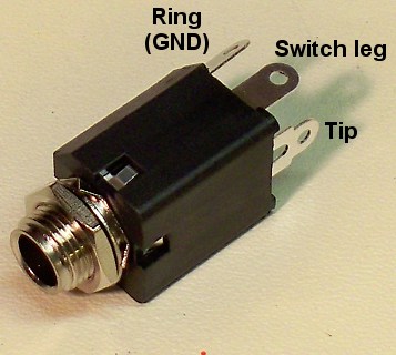
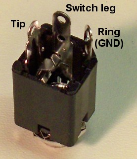
1/4" Phone Jack with NC Switch to Tip Contactor
The unit's amplifier is bypassed when a phone plug is inserted into the line out jack. You must use a jack that has a normally closed switch to the tip contactor. There are several styles of jack. This Amphenol jack (Amphenol Part# ACJM-MVS-2S) is currently shipping in kits. It is always best to ring out whatever jack you use with your multi-meter to make sure of which terminal is which. Don't let the normally closed switch fool you as to which terminal is the tip. Stick a piece of paper between the switch leg and the jack to open the connection while ringing out the jack.
 |
 |
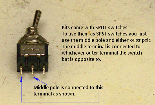
Kits come with SPDT switches which work perfectly as SPST
I send all Single Pole Double Throw Switches in kits because they also serve perfectly as SPST switches. As you can see in this image the switch has three terminals. The middle terminal is common and is connected to either of the outer terminals depending on the position of the switch bat. The terminal that is opposite of the way the switch bat leans is the terminal in contact with the middle terminal. Either outer terminal can be used.
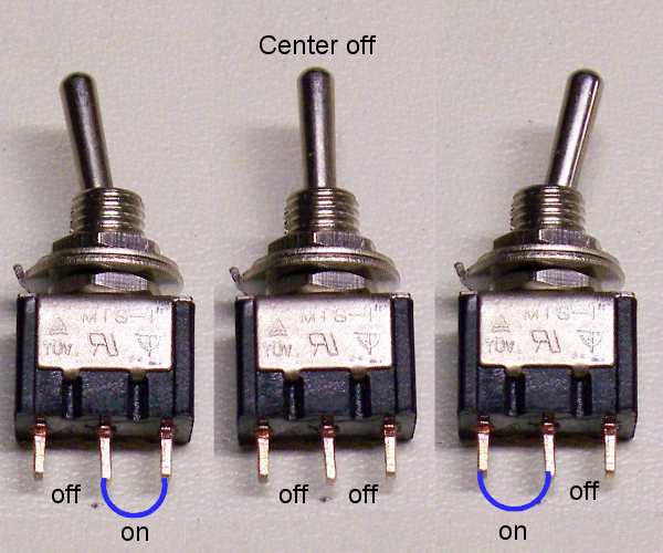
Center off Toggle Switches
Don't confuse your switches. The special center off toggle switches have a center position in which the center pole is not connected to either outer pole. Regular switch bats will go from left to right and will not have a center position. Just click the switches and find the ones that have the center off position.
 |
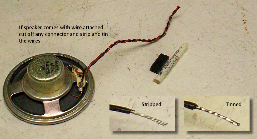
Speaker Lead Preparation
If the speaker comes with wires and a connector on the end simply cut the connector off and remove any identifier sleeve (if present and not connected) from the wires and strip and tin the ends. If no wires are attached to the speaker in your kit simply solder wires of length 6 to 8 inches carefully to the speaker terminals. Speakers are not polarized so it makes no difference which terminal goes to which PC board connection. When working with more than one speaker as in a stereo setup it is important for speakers to be connected to the amp so that they are "in phase" so it matters then but not for this project.
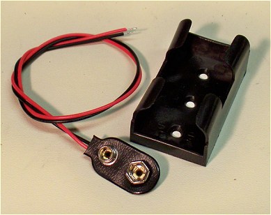
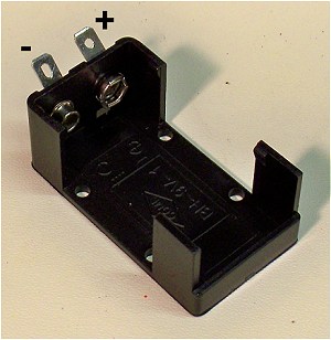
Battery Holder and Battery Snap
Some kits come with a battery holder and separate battery snap with wires while others come with a battery holder with an integrated battery snap and terminals to which you must solder wires to connect to the circuit board and/or front panel. The battery holder with the integrated battery snap is clearly marked as to which terminal is positive and which is negative. I suggest that you use two different colored wires so as not to confuse which is positive and which is negative (red and black would be a good choice). Mount either battery holder using small flat head screws (#6 flat head philips screws work well).
 |
 |
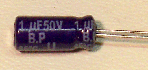
Bipolar or Non-Polarized Caps
Don't confuse your caps. The bipolar (or non-polarized) aluminum caps look kind of like electrolytic caps except they have no + or - markings. Instead the cap is marked B.P.
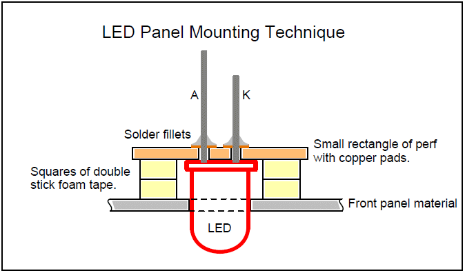
Front Panel LED Mounting
To mount the LED to the front panel I trim a small piece of pre-drilled perf board with copper pads into a small rectangle. The idea is to have perf board "ears" on either side of the LED after it is soldered to the small rectangle of perf board. I then cut double sided foam tape (the stuff that sticks forever) into small squares that I apply to the perf board on both sides of the LED (on the perfboard "ears"). I use a double stack of the foam tape so that the LED sticks through the panel less (you could go three layers if you want). I then push the LED through the panel and the double stick tape holds it in place. I leave the LED leads long so I can solder to them. If you trim them prior to wiring the panel to the PCB BE SURE TO LEAVE THE ANODE LEAD LONGER THAN THE KATHODE so you can tell them apart. I usually trim them when the intra-panel wiring is done.
PC Board Mounting using MFOS NOISE TOASTER Panel
The MFOS NOISE TOASTER Panel has two mounting holes for the PC board. For each mount I used two 1/4" x 3/8" long spacers with 1 1/4" 6-32 machine screws and nuts. I mounted the board with the components away from the plate so that the pots and switches can fit underneath the PC board. I orient the board so that the VCO section is near the VCO controls on the panel. The Parts kit comes with the bolts, nuts and spacers. To get the panel with the parts kit order part number NOISETOASTERPARTSKITANDPANEL (NOISE TOASTER PCB, Parts Kit, Panel) from the catalog.
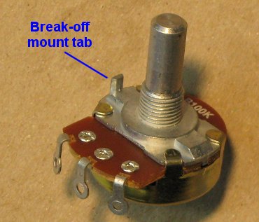
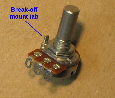
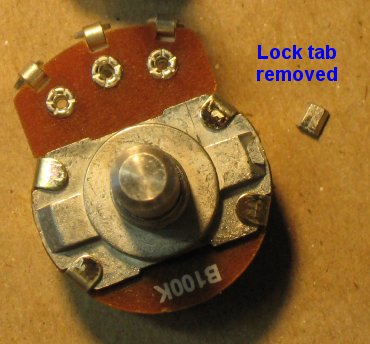
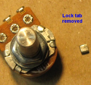
How To Remove Break-off Lock Tabs From Your Potentiometers
| If your pots have little tabs on them you will need to remove them so that you can mount them to your faceplate. It is really easy to do. Carefully snap off the little tab near the pot body and voila it's done. Some kits come with larger pots and some kits come with smaller pots. The smaller pots are at times more expensive than the larger pots. They're all good quality pots and they all work the same way. | |
Regular Sized Pots |
Smaller Sized Pots |
|---|---|
| This is the break-off lock tab which can be used to keep the pot from turning when you turn the pot shaft but tightening the mounting nut works just fine. If you have the wherewithal to drill little holes for these pesky things... be my guest. If not... read on. | |
 |
 |
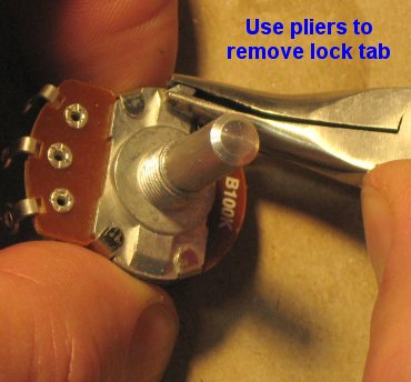
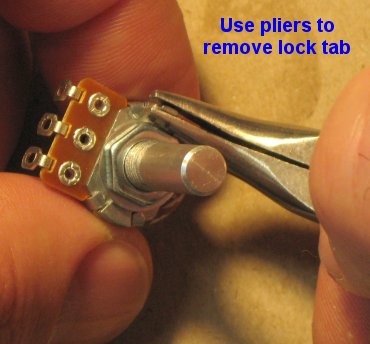
| Using pliers, grasp the tab as low on it as you can and then gently twist the pliers outward. I told you it was easy. | |
 |
 |
| The little broken off tabs look like this. Now you can mount your pot without the little tab getting in the way. | |
 |
 |